
Index 307
Flash_EPROM_programmer
Published:2009/7/24 10:39:00 Author:Jessie

The MAX732 current-mode PWM regulator makes a good flash EPROM programmer because of the logic-compatible shutdown control, and because the supply is capable of programming four flash devices simultaneously. When heavily loaded, the MAX732 operates in the continuous-conduction mode, where inductor current never returns to zero. When inductor current is depleted, the LX voltage rings around the level of the input supply voltage. This is caused by the tank circuit, which is formed by the inductor and stray capacitances (windings, diode, MOSFET within the chip, etc.). Maxim, 1992, Applications and Product Highlights, p. 4-7. (View)
View full Circuit Diagram | Comments | Reading(1549)
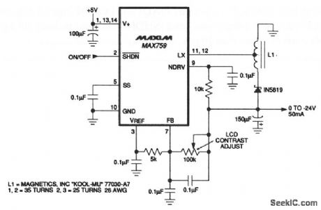
LCD_supply_with_digital_adjust
Published:2009/7/24 10:35:00 Author:Jessie
If the expense of a customized autotransformer (L1, Fig. 6-25) is too high, this low-cost pulse-skipping circuit can be used. In this case, the relatively high output voltage is accommodated via an extemal switch transistor that has 40-V BVCEO specifications. A simple D/A scheme adjusts the output for contrast control and temperature compensation of the LCD. Maxim, 1992, Applications and Product Highlights, p. 4-5. (View)
View full Circuit Diagram | Comments | Reading(606)
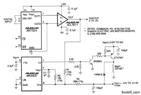
Adjustable_LCD_supply_with_autotransformer
Published:2009/7/24 10:31:00 Author:Jessie
This circuit provides a variable output voltage to adjust the contrast of LCDs. The autotransformer L1 steps up the output to prevent overvoltage to the LX transistor. The total voltage from VIN to LX must be limited to 22 V (with a 5-V input), the voltage at LX cannot exceed -17 V. With L1 (a miniature 0.2-in diameter toroid), the voltage at LX is reduced from the output voltage (determined by the turns ratio). Maxim, 1992, Applications and Product Highlights, p. 4-5. (View)
View full Circuit Diagram | Comments | Reading(529)
8_digit_LED_driver
Published:2009/7/24 10:26:00 Author:Jessie
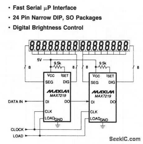
In this circuit, two MAX7217s drive 16 digits from a single 5-V supply, while being addressed through one 3-wire serial link. Only one external component (per chip) is needed. One resistor sets the maximum current (ISET) for all 8 segments, while a fast (up to 10 MHz) cascadable serial interface loads data directly from most microprocessors. Maxim, 1992, Applications and Product Highlights, p. 2-9. (View)
View full Circuit Diagram | Comments | Reading(661)
Isolated_D_A_converters_with_serial_input
Published:2009/7/24 10:24:00 Author:Jessie
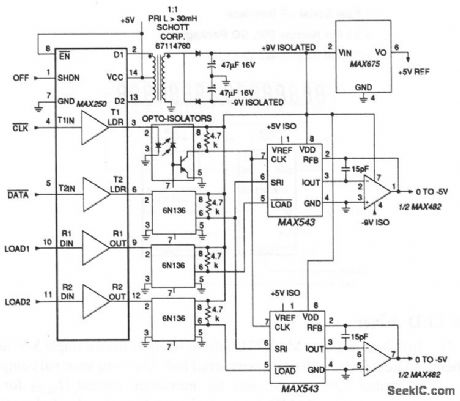
In this circuit, two MAX543 serial-input 12-bit D/A converters (DACs) receive power and data from a MAX250 receiver/transmitter. Clock and data lines are shared by both DACs, but separate LOAD1 and LOAD2 inputs latch the data in. The MAX250 also has a shutdown input (SHDN) that powers down the circuit and cuts supply current to less than 10μA. Maxim, 1992, Applications and Product Highlights, p. 2-9. (View)
View full Circuit Diagram | Comments | Reading(663)
A_D_converter_for_a_41_2_digit_LCD_display
Published:2009/7/24 10:19:00 Author:Jessie
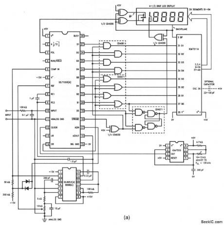
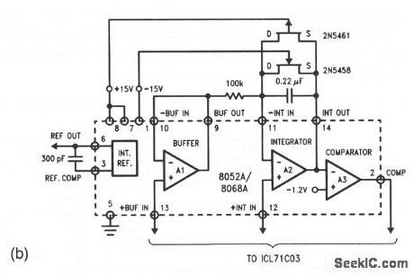
This circuit shows an ICL8052/ICL71C03 chip pair with an ICM7211 driver, which can be used to operate a 41/2-digit LCD display. With the values shown, the full-scale is ±2.000 V. Data bits are latched into the driver by the STROBE signal and Overrange is indicated by blinking the 4 digits. A 120-kHz clock is provided by an ICM7555. Figure 6-22B shows a gross overvoltage protection circuit (to be added if required). If the capacitor is added to put 36 of the ICM7211, the LCD backplane oscillator frequency is reduced from about 150 Hz. To adjust, short terminals 10 and 11 of the ICL71C03 and check that the display is 0000. Then, apply 2.000 V at terminals 10 and 11, and adjust the 10-kΩ potentiometer (pin 7 of the ICL71C03) for a reading of 2000 on the display. Harris Semiconductors, Data Acquisition, 1991, p. 2-25, 2-26. (View)
View full Circuit Diagram | Comments | Reading(2343)
CMOS_driver
Published:2009/7/24 9:36:00 Author:Jessie
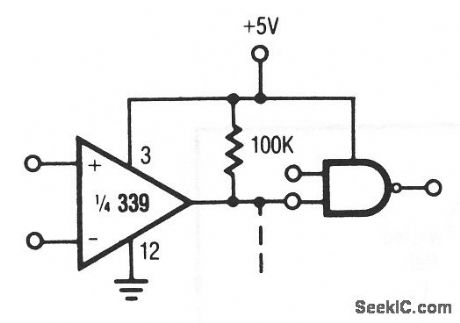
This circuituses a 339 comparator as a CMOS driver. Raytheon Linear Integrated Circuits, 1989, p. 5-30. (View)
View full Circuit Diagram | Comments | Reading(733)
Schmitt_trigger
Published:2009/7/24 9:02:00 Author:Jessie

This circuit is emitter coupled and provides a simple comparator action. The JFET places very little loading on the input. The 2N3565 bipolar is a high hFE transistor, so the circuit has fast transition action and a distinct hysteresis loop. National Semiconductor, Linear Applications Handbook, 1991, p. 118. (View)
View full Circuit Diagram | Comments | Reading(0)
ASTABLE_FLIP_FLOP_WITH_STARTER
Published:2009/6/30 23:47:00 Author:May


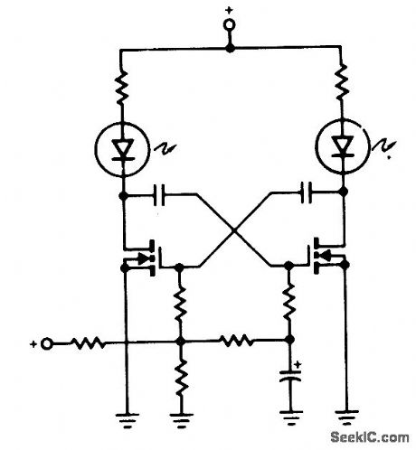
A pair of non-zenered MOSPOWER transistors, a pair of LEDs and a simple RC circuit make an easy sequential flasher with al-most unlimited sequencing time-from mo-mentary to several seconds. The infinite input resistance of the MOSFET gate allows for very long sequencing times that are impossible when using bipolars. One precaution, though, don't wire your circuit using phenolic or printed circuit boards when looking for slow sequencing (they exhibit too much leakage!). (View)
View full Circuit Diagram | Comments | Reading(871)
AUT0_CLOCK
Published:2009/6/30 23:46:00 Author:May
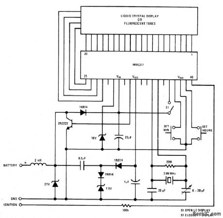
National MM5377 chip for au-tomobile dock interfaces directly with 4-digit Iiquid-crystal or fluorescent-tube display. 12-h format indudes Ieading-zero blanking and colon indication. Voltage-sensitive output drives energy-storage network serving as volt-age doubler/regulator. Crystal oscillator is ref-erence time base.- MOS/LSI Databook, Naˉtional Semiconductor,Santa Clara,CA,1977,1-33-1-37. (View)
View full Circuit Diagram | Comments | Reading(873)
AUDIBLE_DIPPER
Published:2009/6/30 23:45:00 Author:May
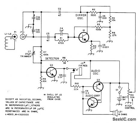
Designed for use by blind radio amateurs, but tone indication has advantage of permitting anyone to concentrate on equipment while checking antenna, tracking parasitics,or neutralizing amplifier with dip meter. Plug-in coils L1-L6 are Heathkit parts 40-1689 through 40-1695. Q1,Q2,and Q4 are Radio Shack RS-2021 or equivalent, and Q3 is RS-2021 or equivalent. Pitch of tone heard from Ioudspeakerdrops sharply when tuned circuit of dip-per becomes Ioaded by extemal source.-W. E.Quay,An Auditory Dip Oscillator, QST,Sept.1978,p25-27. (View)
View full Circuit Diagram | Comments | Reading(1725)
1_Hz_REFERENCE
Published:2009/6/30 23:44:00 Author:May
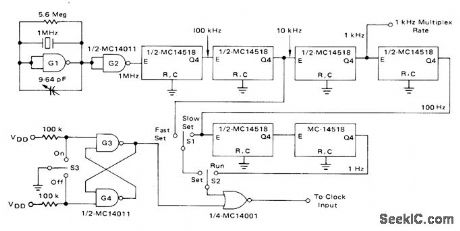
Output of 1-MHz crystal os-cillator is stepped down to 1 Hz by CMOS de-cade divider chain using Motorola MC14518 dual decade counters. Circuit also generates 1-kHz multiplex rate for display used with 24-h in-dustrial dock. Supply is +5 V.-D. Aldridge and A. Mouton, Industrial Clock/Timer Featuring Back-Up Power Supply Operation, Motorola, Phoenix, AZ, 1974, AN-718A, p 5. (View)
View full Circuit Diagram | Comments | Reading(787)
BUFFERED_BREAKOUT_BOX
Published:2009/6/30 23:22:00 Author:May
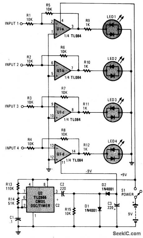


The monitoring circuit consists of four tri-color LEDs driven by an equal number of op amps configured as gain-of-one inverting amplifiers. Each LED is wired in the circuit so that it glows red when the input to the op amp is high, and green when the input is low. The LED remains off when the input is disconnected from a circuit, when it's at ground potential, and when it's connected to a 3-state output that's in the high-impedance state. Each input has an impedance of 10,000 ohms preventing the circuitfrom loading communication lines. The op amp requires both positive and negative sup-ply voltages to properly drive the LEDs. Both voltages are supplied by a single, nine-volt battery. The battery supplies the positive source directly. The negative source is supplied via a CMOS 555 oscillator/timer that's configured as an astable oscillator, which is used to drive a standard diode/capacitor voltage doubler. When the 555 is connected to the monitoring circuit, the output voltage is not 18 volts (2×9), but a little under nine volts, due to loading. The circuit draws about 16 mA with all LEDs off; with all four on, it draws between 20 and 30 mA, depending on how many LEDs are high, and how many are low. The use of CMOS op amps reduces quiescent current drain considerably. (View)
View full Circuit Diagram | Comments | Reading(682)
LOW_CURRENT_CONSUMPTION_LAMP_FLASHER
Published:2009/6/30 23:04:00 Author:May
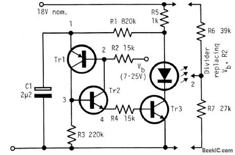
The circuit is economical in components, and will work with virtually any transistors and is reliably self-starting. The voltage Vb can be taken from a divider, as shown at the right. If taken from a fixed source, flashing becomes slower as battery voltage falls.The lowest drive current into the base of Tr3 is about (Vb-0.6 V)/(R2 + R4). Resistor R4 limits the initial current from C1 and, as shown, R2 and R4 can be roughly equal when a divider is used for Vb. Resistor R2 equals R6R7/(R6+ R7). With the voltages shown, and with R2 = R4, the on-time is about 1.1 C1R2 and the off-time about 0.28 C1R1. Using the component values shown the period is about 0.55 sec. with a duty cycle of about 7% and a mean battery current including the Vb divider, about 1.5 mA. (View)
View full Circuit Diagram | Comments | Reading(507)
SERIES_SCR_LAMP_FLASHER_HANDLES_A_WIDE_RANGE_OF_LOADS
Published:2009/6/30 22:56:00 Author:May


Brief full-power flashes are obtained when the SCR conducts during positive half cycles of the line voltage. The SCR fires when the voltage at the divider, R3 and R4, reaches the gate-firing level. Diode D1 conducts during the reverse cycle of the SCR and provides preheating current to the lamp filaments.
(View)
View full Circuit Diagram | Comments | Reading(643)
12_h_WITH_SECONDS
Published:2009/6/30 22:49:00 Author:May

Combination of Mostek clock IC and Sprague high-voltage display drivers, acting through 206C and 216C single in-line resistor network, provides drive for conventional seven-element gas-discharge digital clock display showing hours, minutes, and seconds. Requires -200 V supply. Display can be Burroughs Panaplex, Cherry Plasma-Lux, or Beckman SP series.- Integ rated Circuits Data book-1, Sprague, North Adams, MA 1978, p 3-5.
(View)
View full Circuit Diagram | Comments | Reading(1566)
EIGHT_CHANNEL_MUX_DEMUX_SYSTEM
Published:2009/6/30 22:40:00 Author:May


A number of signals may be sent between two points simultaneously by making a slight modification in the receiver circuit. A second DG508A is used as a demultiplexer, allowing all 8 channels to be monitored continuously. (View)
View full Circuit Diagram | Comments | Reading(519)
MINIATURE_TRANSISTORIZED_LIGHT_FLASHER
Published:2009/6/30 22:36:00 Author:May

R1 adjusts the flash rate. The lamp should be a No. 122, No. 222 or other similar, miniature incandescent lamp. (View)
View full Circuit Diagram | Comments | Reading(539)
PRF_MONITOR_UPPER
Published:2009/6/30 22:35:00 Author:May

Upper channel latches when pulse repetition frequency of train of pulses is higher than specified limits,turning on abovelimit LED driven by JK fip-flop FF1. Lower channel latches and turns on its LED when PRF is below second specified limit, Upper channel als detects single noise pulse,while lower channel detects single missing pulse,After offlimit indication,circuit must be reset.-L.Bilkwood and D.Porat、PRF Monitor with Adjustable End Limits、EDN/EE Magazine,Feb.1、1972,p57-58
(View)
View full Circuit Diagram | Comments | Reading(598)
8_BIT_μP_BUS_INTERFACE
Published:2009/6/30 22:28:00 Author:May

with this double latch technique,valid data will be latched to the DAC until updatedwith the E2 pulse,Timing Will depend on the processor used。 (View)
View full Circuit Diagram | Comments | Reading(514)
| Pages:307/471 At 20301302303304305306307308309310311312313314315316317318319320Under 20 |
Circuit Categories
power supply circuit
Amplifier Circuit
Basic Circuit
LED and Light Circuit
Sensor Circuit
Signal Processing
Electrical Equipment Circuit
Control Circuit
Remote Control Circuit
A/D-D/A Converter Circuit
Audio Circuit
Measuring and Test Circuit
Communication Circuit
Computer-Related Circuit
555 Circuit
Automotive Circuit
Repairing Circuit