
Amplifier Circuit
Index 127
Alternate_amplifier_with_±120_V_output
Published:2009/7/23 23:37:00 Author:Jessie
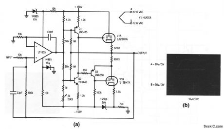
This circuit is similar to that of Fig .1-13, except that vacuum tubes (yes, they still exist ) are used at the output .The full-power band width is 12-kHz with a slew rate of about 12V/μs ,Figure 1-14B shows the results with a ±12-V input (trace A).Danger! this circuit involves high voltages! (View)
View full Circuit Diagram | Comments | Reading(813)
fast_dc_stabilized_inverting_amplifier
Published:2009/7/23 23:48:00 Author:Jessie
This circuit is similar to that of Fig. 1-21, except that the output is inverted, and the summing-point bias-current is low. Figure 1-22B shows operating waveforms for a 10-V output (trace A input, trace B output). Slew rate is about 100 V/μs, with full power bandwidth of 1 MHz. Output current is about 100 mA. (View)
View full Circuit Diagram | Comments | Reading(603)
ISOLATED_PREAMP
Published:2009/7/3 3:20:00 Author:May
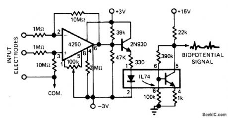
Optoisolator in electrocardiograph preamp circuit prevents circulating ground currents from shocking patients under test. Can be used with practically all other types of AC line-operated equipment in medical en vironments.-R. R. Ady, Let's Take an Illuminating Look at Latest Developments in LED's, EDN Magazine, Aug. 5, 1975, p 30-35. (View)
View full Circuit Diagram | Comments | Reading(623)
Amplifier_with_±100_V_output_15_V_supply
Published:2009/7/23 23:40:00 Author:Jessie
This amplifier provides a ±100-V output, using ±15-V supplies. The bandwidth is 150 Hz with a slew rate of 0.1 V/μs. Output current is 150 mA. Danger! this circuit involves high voltages!
(View)
View full Circuit Diagram | Comments | Reading(528)
COMPLETE_2_W_SERVO_AMPLIFIER
Published:2009/7/23 23:40:00 Author:Jessie
Includes direct-coupled preamplifier and driver stages, with considerable d-c feedback to stabilize bias conditions. Voltage gain of amplifier with feedback loop closed is 10,000. Overall efficiency is 50%. Input impedance is 10,000 ohms and output impedance is 150 ohms.-Texas Instruments Inc., Transistor Circuit Design, McGraw-Hill, N.Y., 1963, p 247. (View)
View full Circuit Diagram | Comments | Reading(1004)
±15_V_CHOPPER_AMPLIFIER
Published:2009/7/3 3:17:00 Author:May
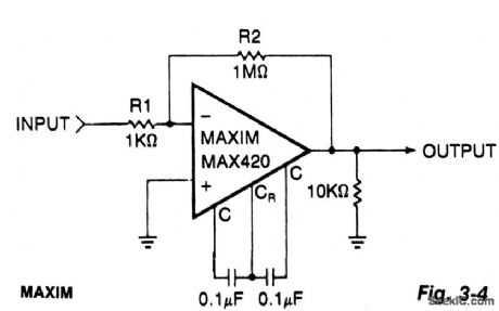
This simple circuit is a gain-of-1000 inverting amplifier. It will amplify submillivolt signals up to signal levels suitable for further processing. In almost all system applications, it is best to use as much gain as possible in the MAX420, thus minimizing the effects of later-stage offsets. For exam-ple, if circuitry following the MAX420 has an offset of 5 mV, the additional offset referred back to the MAX420 input (gain = 1000) will be 5μV, doubling the system's offset error. (View)
View full Circuit Diagram | Comments | Reading(580)
Amplifier_with_1000_V_output_28_V_supply
Published:2009/7/23 23:38:00 Author:Jessie
This unipolar-output amplifier swings 1000 V and supplies 15 W. The boost stage operates from a 28-V supply. Figure 1-15B shows the results with a±10-V input (trace A). Bandwidth is about 60 Hz. Danger! this circuit involves high voltages ! (View)
View full Circuit Diagram | Comments | Reading(513)
ABSOLUTE_VALUE_NORTON_AMPLIFIER
Published:2009/7/3 3:04:00 Author:May
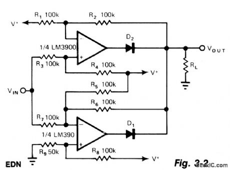
The noninverting amplifter has a gain of R2/R3 (1 in this case) and produces a voltage of Vout during a positive excursion of Vin with respect to ground.The inverting amplifter accommodates the negative excursions of Vin; its gain is given by -R6/R7, which equals -1 to maintain symmetry with the noninverting amplifter. R9 provides adjustment for the symmetry, supply variations, and offsets. Even though the circuit operates on a single supply, Vin can go negative to the same extent that it goes positive. (View)
View full Circuit Diagram | Comments | Reading(787)
INPUT_OUTPUT_BUFFER_AMPLIFIER_FOR_ANALOG_MULTIPLEXERS
Published:2009/7/3 3:03:00 Author:May
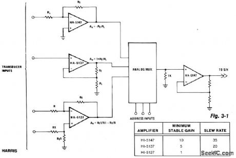

The precision input characteristics of the HA-5147 help simplify system error budgets, while its speed and drive capabilities provide fast charging of the multiplexer's output capacitance. This speed eliminates an increased multiplexer acquisition time, which can be induced by more limited amplifiers. The HA-5147 accurately transfers information to the next stage while effectively reducing any loading effects on the mul-tiplexer's output. (View)
View full Circuit Diagram | Comments | Reading(584)
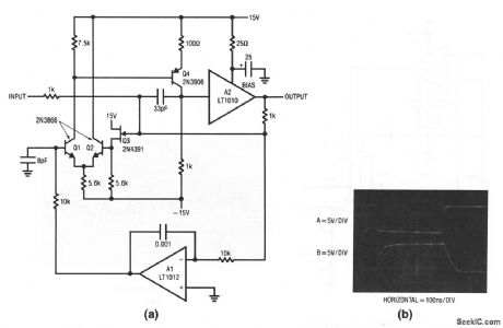
Fast_dc_stabilized_noninverting_amplifier
Published:2009/7/23 23:46:00 Author:Jessie
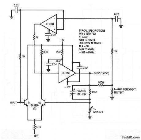
This circuit combines an LT1010 (and a fast discrete stage) with an LT1008-based dc-stabilizing loop. The output depends on the setting of the gain pot. Typical specifications are shown for voltage gains of 2 and 10. The normal tendency of the Q1/Q2 stage to drift is corrected by the LT1008. This correction stage is similar to those of Figs. 1-19 and 1-20, except that the feedback is taken from a divided-down sample of the fast amplifier. The ratio of this divider should be set (by the selection of the gain-dependent resistor) to the same value as the circuit closed-loop gain (typically 2 or 10). The output is typically 1 VPP (suitable for video), and should be adjusted for optimum (with a load applied) using the peaking capacitor.
(View)
View full Circuit Diagram | Comments | Reading(612)
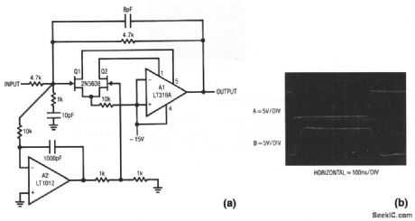
Gain_trimmable_wideband_FET_amplifier
Published:2009/7/23 23:45:00 Author:Jessie
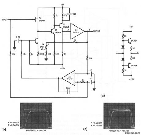
This circuit is similar to that of Fig. 1-19, except that voltage gain can be trimmed (to full unity gain, or to a gain of 10, etc.). With a 1-kΩ gain adjust set to unity, power bandwidth (1 Vpp) is 10 MHz, and slew rate is 100 V/μs. With the voltage gain set at 10, power bandwidth stays at 10 MHz, while the -3-dB point drops to about 22 MHz (from about 35 MHz at unity gain). With the optional discrete stage, slew rate exceeds 1000 V/μs, full power bandwidth is 18 MHz, and the -3-dB point is 58 MHz. With a voltage gain of 10, full power is available to 10 MHz, with the -3-dB point at 36 MHz. Figures 1-20B and 1-20C show the response with the LT1010 output, and the discrete output, respectively. As shown, the discrete stage is slightly faster (less delay between input and output). (View)
View full Circuit Diagram | Comments | Reading(767)
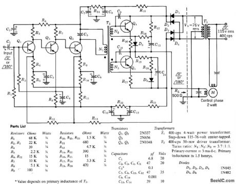
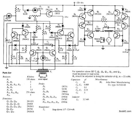
60_CPS_SERVO_AMPLIFIER
Published:2009/7/23 23:45:00 Author:Jessie
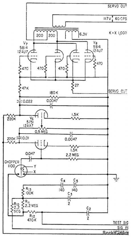
Consists of 60-cps d-c chopper, two stages of 60-cps voltage amplification V6, and 4-W power output stage V7-V8 that drives control winding of two-phase servo motor. Over-all power gain is 80 db.-P. G. Balko, Infrared Finds Audio Suspension Leaks, Electronics, 31:49, p 82-85. (View)
View full Circuit Diagram | Comments | Reading(591)
Fast_dc_stabilized_composite_amplifier
Published:2009/7/23 23:42:00 Author:Jessie
This composite amplifier is similar to that of Fig. 1-17, except that FETs are used to increase speed. Full power bandwidth is about 1 MHz, with a slew rate over 100 V/μs. Input bias is about 100 pA, offset and drift are about the same as Fig. 1-17. Figure 1-18B shows pulse response (trace A is input, trace B output).
(View)
View full Circuit Diagram | Comments | Reading(543)
Basic_dc_stabilized_composite_amplifier
Published:2009/7/23 23:41:00 Author:Jessie
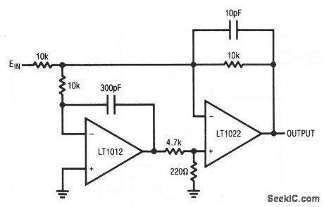
This composite amplifier combines the LT1012's 35-μV offset and 1.5 V/℃ drift, with the LT1022's 24 V/μs slew rate and 300-kHz full power bandwidth, to provide both high speed and low drift/offset. Input bias is about 100 pA. (View)
View full Circuit Diagram | Comments | Reading(633)
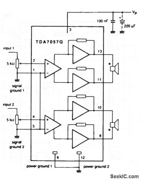
Low_voltage_compandor
Published:2009/7/24 0:01:00 Author:Jessie

This single-chip circuit operates on voltages from 3 V to 7V, with a reference voltage (pin 8) of 100 mV for 0 dB. There is one dedicated summing op amp per channel, and two extra uncommitted op amps. The output can drive 600Ω. (View)
View full Circuit Diagram | Comments | Reading(1156)
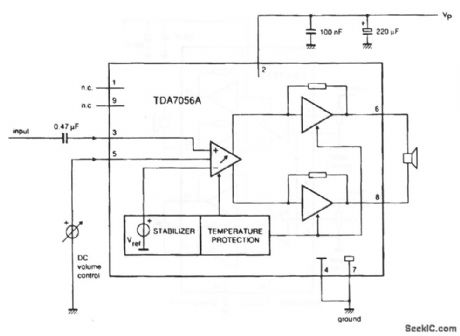
Single_chip_audio_amplifier_BTL_stereo_3_W
Published:2009/7/24 Author:Jessie
This circuit is similar to that of Fig. 1-27, except that no built-in volume control is provided, and two (stereo) channels are available. The supply range is from 3 V to 18 V. The circuit provides a 3-W per channel output, with an 11-V supply, into 16-Ω loads. Fixed, closed-loop voltage gain is 39 dB (1-V supply, 16-Ω load). (View)
View full Circuit Diagram | Comments | Reading(1029)
Single_chip_audio_amplifier_BTL_mono_3_W
Published:2009/7/23 23:59:00 Author:Jessie
This circuit is similar to that of Fig. 1-27, except that no built-in volume control is provided. The supply range is from 3 V to 18 V. The circuit provides an output of 3 W, with an 11-V supply, into a 16-Ωload. Fixed, closed-loop voltage gain is 39 dB (11-V supply, 16-Ω load). (View)
View full Circuit Diagram | Comments | Reading(810)
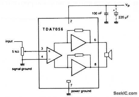
Single_chip_audio_amplifier_BTL_3_W_with_volume_control
Published:2009/7/23 23:59:00 Author:Jessie
This circuit is similar to that of Fig. 1-27, except that the output is 3.4 W with a 12-V supply, into a 16-Ω load (View)
View full Circuit Diagram | Comments | Reading(858)
SWITCHING_MODE_SERVO_AMPLIFIER
Published:2009/7/23 23:58:00 Author:Jessie
Input signal is used to control duration of relatively constant repetition-rate pulse signal, to give pulse-duration modulation. Repetition rote is 10 kc. Switching-mode output stage supplies power to control winding of two-phase servo motor.-Texas Instruments Inc., Transistor Circuit Design, McGraw-Hill, N.Y., 1963, p 483. (View)
View full Circuit Diagram | Comments | Reading(1782)
VARIABLE_Q_AF
Published:2009/7/3 2:28:00 Author:May


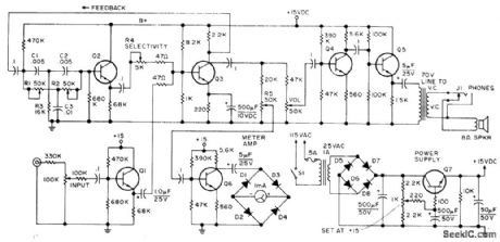

Consists of tuned amplifier having inverse feedback, connected so bandwidth at -6 dB is variablefrom 50 to 400 Hz for center frequency of 1 kHz. Improves selectivity of amateur receivers. Audio from receiver is applied to inverter Q3 through Q1. Part of inverted signal is fed back to twin-T network R1-R2-R3-C1-C2-C3 which has high impedance to ground except at its resonant frequency. Unattenuated signal goes through Q2 for adding to uninverted output at base of Q3. Degree of cancellation by two out-of-phase signals feeding Q3 is controned by R4 to adjust selectivity Filtered output is boosted by Q4 and Q5,Article covers construction,calibration,and operation,Q1-Q6 are GE-20,and Q7 is GE-14 or GE-28,-c,Townsend,A Variable Q Audio Fillter,73 Magazine,Feb,1974, p 54-56. (View)
View full Circuit Diagram | Comments | Reading(625)
| Pages:127/250 At 20121122123124125126127128129130131132133134135136137138139140Under 20 |
Circuit Categories
power supply circuit
Amplifier Circuit
Basic Circuit
LED and Light Circuit
Sensor Circuit
Signal Processing
Electrical Equipment Circuit
Control Circuit
Remote Control Circuit
A/D-D/A Converter Circuit
Audio Circuit
Measuring and Test Circuit
Communication Circuit
Computer-Related Circuit
555 Circuit
Automotive Circuit
Repairing Circuit