
Index 118
PROTECTIVE_DIODES_FOR_SCHMITT_TRIGGER
Published:2009/7/23 21:25:00 Author:Jessie
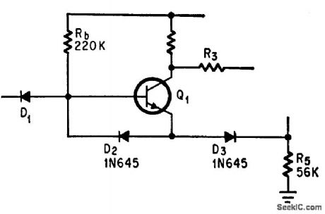
Addition of diodes D2 and D3 to modified Schmitt trigger having isolating diode D1 prevents reverse breakdown of emittor-base junction of Q1.-J. Gaon, Diode and Resistor Increase Input Resistance of Schmitt, Electronics, 39:12, p 110-111. (View)
View full Circuit Diagram | Comments | Reading(608)
True_logarithmic_IF_amplifier
Published:2009/7/23 21:25:00 Author:Jessie
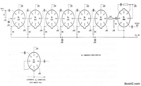
The SL531 shown here is a wide-band amplifier for use in IF circuits or strips ofthe true log type(where input and output are at the same frequency and nodetection Occurs) With the values shown,the frequency range is 10 to 200 MHz.An SL560 is used as a unity-gain buffer, the output of the log strip being attenuated before the SL560 to give a nominal 0-dBm output into 50Ω. The low-level gain is 60 dB with an output dynamic range of 20 dB. (View)
View full Circuit Diagram | Comments | Reading(653)
PNPN_SHIFT_REGISTER
Published:2009/7/23 21:24:00 Author:Jessie
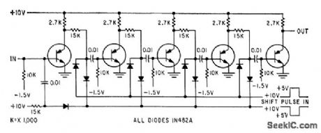
Consists of five one bit memory elements connected in cascade.-J. B. Hangstefer and L. H. Dixon, Jr., Triggered Bistable Semiconductor Circuits, Electronics, 32:35, p 58-60. (View)
View full Circuit Diagram | Comments | Reading(541)
TYPICAL_SCHMITT_TRIGGER
Published:2009/7/23 21:21:00 Author:Jessie
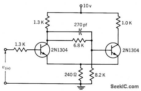
Performs well at frequencies up to 100 kc. Capacitor may be removed for low-frequency operation. Widely used to produce square wave from sinusoidal input, because regenerative circuit changes states abruptly when input signal crosses specific d-c triggering levels.-Texas Instruments Inc., Transistor Circuit Design, McGraw-Hill, N.Y., 1963, p 382. (View)
View full Circuit Diagram | Comments | Reading(830)
SIMPLIFIED_UJT_SCR_TRIGGER
Published:2009/7/23 21:30:00 Author:Jessie
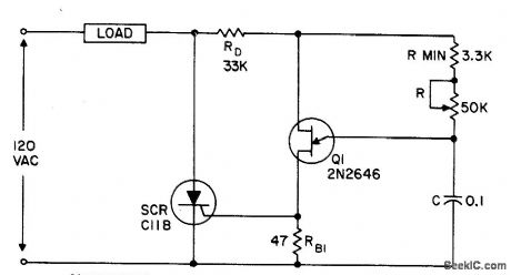
Emitter timing circuit and base-2 of ujt are supplied directly from ac line, with dropping resistor RD keeping peak voltage on ujt within specifications.- Transistor Manual, Seventh Edition, General Electric Co., 1964, p 329. (View)
View full Circuit Diagram | Comments | Reading(1990)
Low_noise_preamplifier
Published:2009/7/23 21:29:00 Author:Jessie

Figure 2-5A shows an SL560 used as a preamplifier.Figure 2-5B shows the typical frequency response. (View)
View full Circuit Diagram | Comments | Reading(587)
500_KC_SCHMITT_TRIGGER
Published:2009/7/23 21:29:00 Author:Jessie

Used for wave form restoration, signal level shifting, squaring, and d-c level detection. Q1 conducts if input is more negative than -5 v. Q2 conducts when input is more positive than -2 v. Operating range is -55 to 71℃.- Transistor Manual, Seventh Edition, General Electric Co., 1964, p 200. (View)
View full Circuit Diagram | Comments | Reading(682)
Analog_multiplier
Published:2009/7/23 21:29:00 Author:Jessie


The output of this circuit is equal to input A times input B times 100, using the values shown. (View)
View full Circuit Diagram | Comments | Reading(0)
Low_noise_wideband_amplifier_with_AGC
Published:2009/7/23 21:28:00 Author:Jessie

This circuit combines an SL550 (amplifier with external gain control) and an SL560 (low-noise amplifier) to form a very simple wideband amplifier with AGC. (View)
View full Circuit Diagram | Comments | Reading(746)
Input_amplifier_for_a_4_1_2_digit_voltmeter_
Published:2009/7/23 21:27:00 Author:Jessie

This circuit provides an approximate 10-MΩ input impedance, and can be used with any 1-V full-scale A/D converter. (View)
View full Circuit Diagram | Comments | Reading(651)
Basic_inverting_amplifier
Published:2009/7/23 21:34:00 Author:Jessie

This circuit shows an LM107 that is connected in the classic inverting-amplifier configuration, where VOUT is opposite to VIN (if VIN goes positive, VOUT goes negative, and vice versa). The amplitude of the output depends on the ratio of R1 and R2 (within the limits of the supply voltage), and R3 is selected to equal the parallel resistance of R1 and R2. (View)
View full Circuit Diagram | Comments | Reading(525)
N_STAGE_RING_COUNTER
Published:2009/7/23 21:32:00 Author:Jessie

Uses modified memory circuit, in which input pulse turns off all pnpn stages except that following on stage.-J. B. Hangstefer and L.H. Dixon, Jr., Triggered Bistable Semiconductor Circuits, Electronics, 32:35, p 58-60. (View)
View full Circuit Diagram | Comments | Reading(668)
Tracking_positive_and_negative_voltage_references
Published:2009/7/23 21:32:00 Author:Jessie

This circuit provides both positive and negative that remain constant, in spite of changes in source voltage or VS. (View)
View full Circuit Diagram | Comments | Reading(549)
Low_noise_high_gain_amplifier
Published:2009/7/23 21:31:00 Author:Jessie

Figure 2-7A shows an SL560 used as a direct-coupled-coupled high-gain amplifier. Figure 2-7B shows the typical frequency response. (View)
View full Circuit Diagram | Comments | Reading(465)
POWER_FLIP_FLOP
Published:2009/7/23 21:31:00 Author:Jessie

Delivers square wave output pulse of 1 amp when pnpn unit is triggered on by low-level positive pulse applied to its base.-J. B. Hangstefer and L. H. Dixon, Jr., Triggered Bistable Semiconductor Circuits, Electronics, 32:35, p 58-60. (View)
View full Circuit Diagram | Comments | Reading(720)
Precision_current_monitor
Published:2009/7/23 21:30:00 Author:Jessie


This circuit produces an output voltage that is proportional to the current that is applied to the load RL. (View)
View full Circuit Diagram | Comments | Reading(631)
Low_noise_wide_bandwidth_ampliffer
Published:2009/7/23 21:30:00 Author:Jessie

Figure 2-6A shows an SL560 used as a wide-bandwidth amplifier.Figure 2-6B shows the bypical frequency response. (View)
View full Circuit Diagram | Comments | Reading(533)
AFC_FOR_F_M_TUNER
Published:2009/7/23 21:43:00 Author:Jessie

Obtained by amplifying change in output from ratio detector as caused by local oscillator drift, and applying resulting error signal to voltage-tunable ferroelectric capacitor in local oscillator through d-c amplifier,-T. W. Butler, Jr., Ferroelectrics Tune Electronic Circuits, Electronics, 32:3, p 52-55. (View)
View full Circuit Diagram | Comments | Reading(580)
TV_AUDIO_AMPLIFIER
Published:2009/7/6 2:10:00 Author:May

The amplifier picks up the TV's audio output signal and amplifies it to drive a set of earphones for private listening. It is built around an LM324 quad op amp and an LM386 low-power audio amplifier. The circuit uses an inexpensive electret microphone element as the pick-up and a set of earphones as the output device. (View)
View full Circuit Diagram | Comments | Reading(3410)
SPEAKER_AMPLIFIER_FOR_HAND_HELD_TRANSCEIVERS
Published:2009/7/6 2:08:00 Author:May

The LM383 is an audio-power amplifier that is capable of producing up to 8W of audio output. R1 is essentially a load resistor for the hand-held transceiver's audio output. R2 can be composed of two fixed resistors in a 10:1 divider arrangement, but using a potentiometer makes it easy to set the amplifier's maximum gain. When powered from a vehicle's electrical system, the amplifier's +12V power source requires filter L1 to eimtnate alternator whine. The LM383 can be mounted directly on the heatsink because the mounting tab is at ground potential. (View)
View full Circuit Diagram | Comments | Reading(748)
| Pages:118/250 At 20101102103104105106107108109110111112113114115116117118119120Under 20 |
Circuit Categories
power supply circuit
Amplifier Circuit
Basic Circuit
LED and Light Circuit
Sensor Circuit
Signal Processing
Electrical Equipment Circuit
Control Circuit
Remote Control Circuit
A/D-D/A Converter Circuit
Audio Circuit
Measuring and Test Circuit
Communication Circuit
Computer-Related Circuit
555 Circuit
Automotive Circuit
Repairing Circuit