
Circuit Diagram
Index 217
Butler Oscillator
Published:2013/1/4 20:27:00 Author:muriel | Keyword: Butler Oscillator
View full Circuit Diagram | Comments | Reading(1488)
ICL7641/7642 four CMOS operational amplifier and its pin main characteristics
Published:2013/1/4 2:07:00 Author:Ecco | Keyword: four CMOS , operational amplifier , pin main characteristics
10mV Input offset voltage; 20μV / ℃ temperature drift; 1pA bias current; Gain Bandwidth GB = 480kHz; conversion rate 160mV/μs; 1nV / √ ˉ Hz ( 1kHz) noise; 400μA Current consumption; ± 1 to ± 9V power supply; ( V +0.30 ~~ ( - v- 0.3) V Total mode input voltage.
(View)
View full Circuit Diagram | Comments | Reading(790)
ICL8007 / A JFET input op amp and its pin main characteristics
Published:2013/1/4 2:13:00 Author:Ecco | Keyword: JFET input op amp , pin main characteristics
10mV Input offset voltage; 50μV / ℃ temperature drift; 500pA bias current; Gain Bandwidth GB = 1MHz; 5V/μs conversion rate; 3.4mA Current consumption; ± 18V power supply; ± 30V differential-mode input voltage; ± 15V common-mode input voltage; 500mW power.
(View)
View full Circuit Diagram | Comments | Reading(828)
ICL8021 programmable operational amplifier and its pin main characteristics
Published:2013/1/4 2:18:00 Author:Ecco | Keyword: programmable operational amplifier, pin main characteristics
2mV Input offset voltage; 5μV /℃ temperature drift; 5nA bias current; Gain Bandwidth GB = 370kHz; 160mV/μs conversion rate; 30μA current consumption; ± 1 to ± 18V power supply; ± 15V differential-mode input voltage; ± 15V common-mode input voltage; 300mW allows loss.
(View)
View full Circuit Diagram | Comments | Reading(711)
ICL8022 dual programmable op amp and its main pin characteristics
Published:2013/1/4 1:20:00 Author:Ecco | Keyword: dual , programmable op amp, main pin characteristics
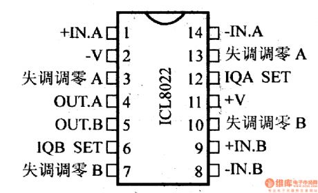
It is same with ICL8021.
(View)
View full Circuit Diagram | Comments | Reading(623)
INA117 precision instrumentation amplifier and its pin main characteristics
Published:2013/1/4 1:34:00 Author:Ecco | Keyword: precision instrumentation amplifier , pin main characteristics
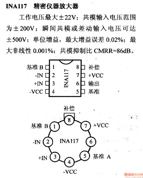
Maximum working voltage is ± 22V; common-mode input voltage range is ± 200V; instant common mode or differential input voltage is up to ± 500V; unity gain maximum gain error is 0.02%; largest nonlinear is 0.001%; common-mode rejection ratio CMRR = 86dB.
(View)
View full Circuit Diagram | Comments | Reading(952)
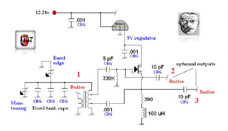
2.8 - 10.5 MHz Signal Generator 4
Published:2013/1/3 20:28:00 Author:muriel | Keyword: 2.8 - 10.5 MHz, Signal Generator
View full Circuit Diagram | Comments | Reading(779)
2.8 - 10.5 MHz Signal Generator 3
Published:2013/1/3 20:27:00 Author:muriel | Keyword: 2.8 - 10.5 MHz, Signal Generator

View full Circuit Diagram | Comments | Reading(714)
2.8 - 10.5 MHz Signal Generator 2
Published:2013/1/3 20:27:00 Author:muriel | Keyword: 2.8 - 10.5 MHz, Signal Generator

View full Circuit Diagram | Comments | Reading(966)
2.8 - 10.5 MHz Signal Generator
Published:2013/1/3 20:26:00 Author:muriel | Keyword: 2.8 - 10.5 MHz, Signal Generator

View full Circuit Diagram | Comments | Reading(854)
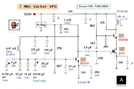
Vackar VFO 2
Published:2013/1/3 20:25:00 Author:muriel | Keyword: Vackar VFO

View full Circuit Diagram | Comments | Reading(1918)
Vackar VFO
Published:2013/1/3 20:25:00 Author:muriel | Keyword: Vackar VFO
View full Circuit Diagram | Comments | Reading(0)
common gate JFET amplifier
Published:2013/1/3 20:24:00 Author:muriel | Keyword: common gate , JFET amplifier
View full Circuit Diagram | Comments | Reading(1230)
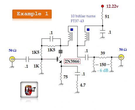
Common Base RF Amps 3
Published:2013/1/3 20:23:00 Author:muriel | Keyword: Common Base, RF Amps
View full Circuit Diagram | Comments | Reading(876)
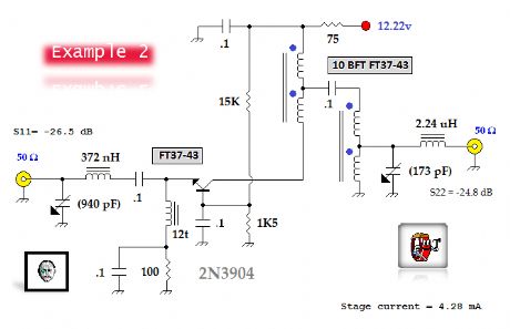
Common Base RF Amps 2
Published:2013/1/3 20:23:00 Author:muriel | Keyword: Common Base, RF Amps
View full Circuit Diagram | Comments | Reading(1041)
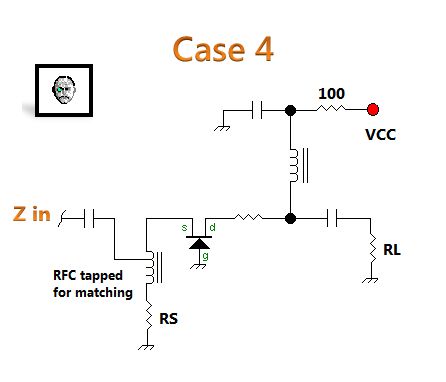
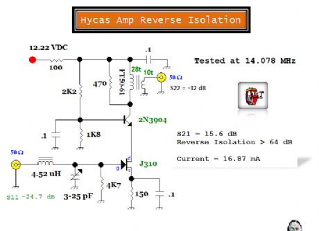
Common Base RF Amps
Published:2013/1/3 20:22:00 Author:muriel | Keyword: Common Base, RF Amps
View full Circuit Diagram | Comments | Reading(1032)
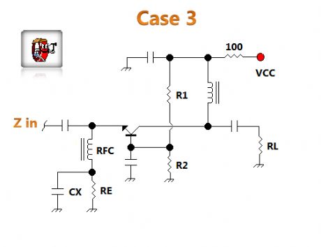
common base bipolar amp
Published:2013/1/3 20:22:00 Author:muriel | Keyword: common base, bipolar amp
View full Circuit Diagram | Comments | Reading(812)
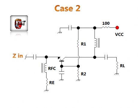
Common Base Amplifiers
Published:2013/1/3 20:21:00 Author:muriel | Keyword: Common Base, Amplifiers
View full Circuit Diagram | Comments | Reading(772)
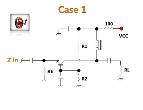
Feedback amplifier
Published:2013/1/3 20:20:00 Author:muriel | Keyword: Feedback amplifier
View full Circuit Diagram | Comments | Reading(668)
forward power gain 2
Published:2013/1/3 20:20:00 Author:muriel | Keyword: forward power gain
View full Circuit Diagram | Comments | Reading(622)
| Pages:217/2234 At 20201202203204205206207208209210211212213214215216217218219220Under 20 |
Circuit Categories
power supply circuit
Amplifier Circuit
Basic Circuit
LED and Light Circuit
Sensor Circuit
Signal Processing
Electrical Equipment Circuit
Control Circuit
Remote Control Circuit
A/D-D/A Converter Circuit
Audio Circuit
Measuring and Test Circuit
Communication Circuit
Computer-Related Circuit
555 Circuit
Automotive Circuit
Repairing Circuit