
Circuit Diagram
Index 206
FOUR QUADRANT SINE GENERATOR
Published:2013/1/10 21:33:00 Author:muriel | Keyword: FOUR QUADRANT , SINE GENERATOR

View full Circuit Diagram | Comments | Reading(792)
High accuracy RPM measurement
Published:2013/1/10 21:31:00 Author:muriel | Keyword: High accuracy, RPM measurement

View full Circuit Diagram | Comments | Reading(1033)
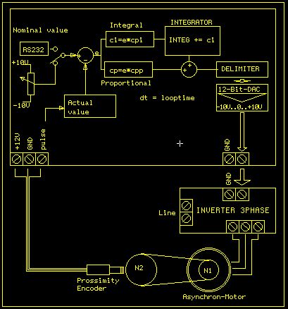
PID Motor control circuit
Published:2013/1/10 21:31:00 Author:muriel | Keyword: PID Motor, control circuit
View full Circuit Diagram | Comments | Reading(720)
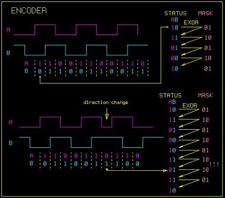
The HC11 read the encoder
Published:2013/1/10 21:30:00 Author:muriel | Keyword: HC11, encoder
View full Circuit Diagram | Comments | Reading(818)
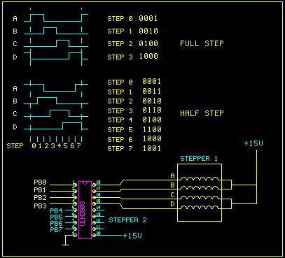
The HC11 controls the stepper
Published:2013/1/10 21:24:00 Author:muriel | Keyword: HC11 , stepper
View full Circuit Diagram | Comments | Reading(622)
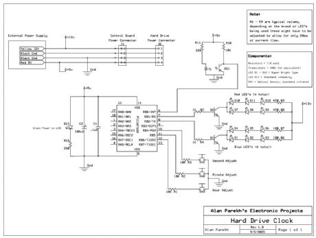
STEPS TO CONSTRUCT CLOCK
Published:2013/1/10 21:23:00 Author:muriel | Keyword: STEPS TO CONSTRUCT CLOCK
View full Circuit Diagram | Comments | Reading(733)
LINE POWERED 60Hz CLOCK GENERATOR
Published:2013/1/10 21:20:00 Author:muriel | Keyword: LINE POWERED , 60Hz, CLOCK GENERATOR
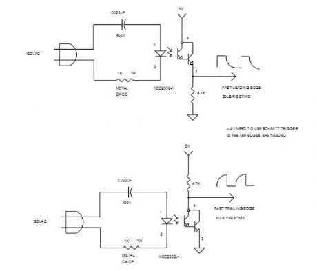
View full Circuit Diagram | Comments | Reading(720)
DC-DC converter
Published:2013/1/10 21:18:00 Author:muriel | Keyword: DC-DC converter

View full Circuit Diagram | Comments | Reading(0)
Easy Xenon DC-DC Converter
Published:2013/1/10 21:18:00 Author:muriel | Keyword: Easy Xenon, DC-DC Converter

View full Circuit Diagram | Comments | Reading(776)
Six metres on your two metre receiver
Published:2013/1/10 21:16:00 Author:muriel | Keyword: Six metres , two metre receiver
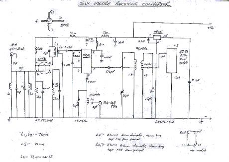
View full Circuit Diagram | Comments | Reading(736)
VHF-HF TRANSVERTER
Published:2013/1/10 21:14:00 Author:muriel | Keyword: VHF-HF TRANSVERTER
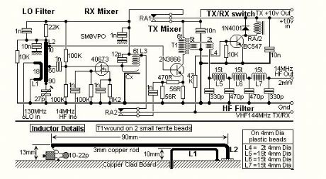
View full Circuit Diagram | Comments | Reading(1888)
PULSE PERIOD TO VOLTAGE CONVERTERS
Published:2013/1/10 21:11:00 Author:muriel | Keyword: PULSE PERIOD, VOLTAGE CONVERTERS

View full Circuit Diagram | Comments | Reading(778)
FM broadcast direct conversion receiver
Published:2013/1/10 21:08:00 Author:muriel | Keyword: FM broadcast, direct conversion receiver

View full Circuit Diagram | Comments | Reading(1244)
Hear Amateurs on your FM Radio
Published:2013/1/10 21:06:00 Author:muriel | Keyword: FM Radio

View full Circuit Diagram | Comments | Reading(1195)
1us Light Pulse Discriminator Plus F to V Converter
Published:2013/1/10 20:35:00 Author:muriel | Keyword: 1us , Light Pulse Discriminator, F to V Converter

View full Circuit Diagram | Comments | Reading(1110)
INA110 high precision JFET input instrumentation amplifier and its pin main characteristics
Published:2013/1/10 3:01:00 Author:Ecco | Keyword: high precision , JFET input, instrumentation amplifier , pin main characteristics

The maximum operating voltage is ± 18V; input voltage range is ± VCC; bias current is less than 50pA; stabilizing time is less than 4μs; common-mode rejection ratio is 106dB; gain can be 1,10,100,200 and 500, and it is convenient to convert; temperature drift voltage is less than 2mV / ℃, pin is compatible with the AD524, AD624.
(View)
View full Circuit Diagram | Comments | Reading(1181)
ISO100 broadband isolation amplifier and its pin main characteristics
Published:2013/1/10 2:46:00 Author:Ecco | Keyword: broadband isolation amplifier , pin main characteristics

The maximum operating voltage is ± 18V; isolation voltage is 2500V; input current range is ± 1mA (Vout / in = RF); leakage current is less than 0.3μA; bandwidth is 60kHz; the total analog rejection ratio CMRR = 90dB; common-mode input voltage is ± 10V; output impedance is 2000000kΩ.
(View)
View full Circuit Diagram | Comments | Reading(856)
ISO106 high pressure isolation buffer amplifier and its pin main characteristics
Published:2013/1/10 2:41:00 Author:Ecco | Keyword: high pressure , isolation buffer amplifier , pin main characteristics

ISO106's performance is same with ISO102, and the main difference has the following two points: 1.ISO106 continuous isolation voltage is 3500V; 2.ISO106 uses 40 -pin DIP package; and the major pin definitions can be found in the ISO102.
(View)
View full Circuit Diagram | Comments | Reading(703)
LM6182 current feedback amplifier and its pin main characteristics
Published:2013/1/10 2:37:00 Author:Ecco | Keyword: current feedback amplifier, pin main characteristics


Operating voltage range is ± 18V or 7.0 ~32V; closed-loop bandwidth is 100MHz; conversion rate is 2000V/μs; differential gain is 0.05%; difference is 0.04 °; output voltage is ± 10V; input offset voltage is 2mV; inverting input bias current is 2μA; noninverting input bias current is 0.75μA; output resistance is 0.2Ω; PSRR = 80dB; CMRR = 60dB; noninverting input resistance is 10MΩ.
(View)
View full Circuit Diagram | Comments | Reading(715)
Dual operational amplifier and its pin main characteristics
Published:2013/1/10 2:14:00 Author:Ecco | Keyword: Dual operational amplifier, pin main characteristics

Input offset voltage is 1mV; bias current is 6nA; Gain Bandwidth Product GB = 3MHz; conversion rate is 1V/μs; noise is 30nV / √ ¯ Hz ( 1kHz); Current consumption is 6mA ; power supply is ± 15V; differential-mode input voltage is ± 32V; common mode input voltage is ± 32V.
(View)
View full Circuit Diagram | Comments | Reading(727)
| Pages:206/2234 At 20201202203204205206207208209210211212213214215216217218219220Under 20 |
Circuit Categories
power supply circuit
Amplifier Circuit
Basic Circuit
LED and Light Circuit
Sensor Circuit
Signal Processing
Electrical Equipment Circuit
Control Circuit
Remote Control Circuit
A/D-D/A Converter Circuit
Audio Circuit
Measuring and Test Circuit
Communication Circuit
Computer-Related Circuit
555 Circuit
Automotive Circuit
Repairing Circuit