
Circuit Diagram
Index 205
LC Meter Based on the AVR ATTINY861
Published:2013/1/15 0:27:00 Author:muriel | Keyword: LC Meter, AVR ATTINY861

View full Circuit Diagram | Comments | Reading(2195)
NJM4560 dual wideband op amp and its pin main characteristics
Published:2013/1/11 1:45:00 Author:Ecco | Keyword: dual wideband op amp , pin main characteristics
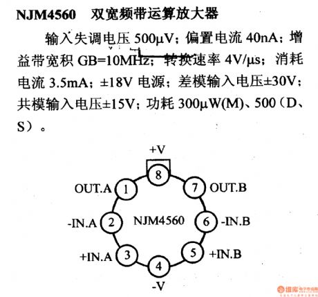
500μV input offset voltage; 40nA bias current; Gain Bandwidth Product GB = 10MHz; 4V/μs conversion rate; 3.5mA current consumption; ± 18V power supply; ± 30V differential-mode input voltage; ± 15V common-mode input voltage; power is 300μW ( M),or 500μW (D, S).
(View)
View full Circuit Diagram | Comments | Reading(3065)
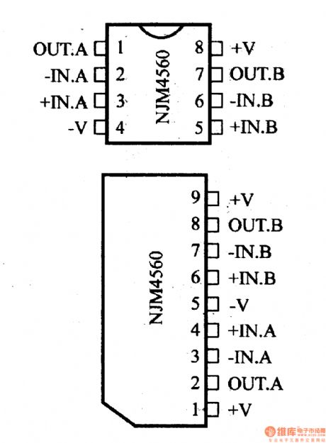
NJM4562 dual low-noise op amp and its pin main characteristics
Published:2013/1/11 1:56:00 Author:Ecco | Keyword: dual low-noise op amp , pin main characteristics
500μV input offset voltage; 200nA bias current; 4V/μs conversion rate; 0.6μVRMS noise; 3.5mA current consumption; ± 18V power supply; ± 30V differential-mode input voltage; ± 15V common-mode input voltage; power is 300μW ( M),or 500μW (D, S, T).
(View)
View full Circuit Diagram | Comments | Reading(956)
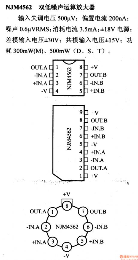
OP-06 high-gain operational amplifier and its pin main characteristics
Published:2013/1/11 2:03:00 Author:Ecco | Keyword: high-gain, operational amplifier , pin main characteristics
60μV input offset voltage; 300nV / ℃ temperature drift; 30nA bias current; 100V/μs conversion rate; 7nV / √ ¯ Hz (1Hz ) noise; 3mA current consumption; ± 22V power supply; ± 30V differential-mode input voltage; ± 22V common-mode input voltage; the gain is high; common-mode rejection ratio and power supply rejection ratio are large; the power consumption is 500mW.
(View)
View full Circuit Diagram | Comments | Reading(607)
OP-07 Low offset operational amplifier and its pin main characteristics
Published:2013/1/11 2:28:00 Author:Ecco | Keyword: Low offset , operational amplifier, pin main characteristics
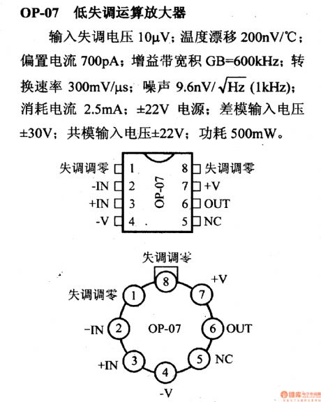
Input offset voltage is 10μV; temperature drift is 200nV / ℃; bias current is 700pA; Gain Bandwidth Product GB = 600kHz; conversion rate is 300mV/μs; the noise is 9.6nV / √ ¯ Hz (1Hz ); Current consumption is 2.5mA ; power supply is ± 22V; differential mode input voltage is ± 30V; common-mode input voltage is ± 22V ; the power is 500mW.
(View)
View full Circuit Diagram | Comments | Reading(795)
OP-37 wide-band high-precision, high - speed operational amplifier and its pin main characteristics
Published:2013/1/11 2:36:00 Author:Ecco | Keyword: wide-band , high-precision, high - speed , operational amplifier, pin main characteristics
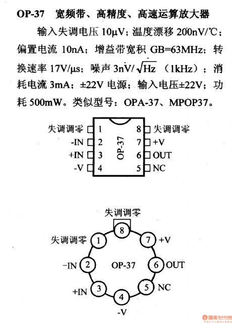
Input offset voltage is 10 μV; temperature drift is 200nV / ℃; bias current is 10nA; Gain Bandwidth Product GB = 63kHz; conversion rate is 17V/μs; noise is 3nV / √ ¯ Hz (1Hz ); Current consumption is 3mA; input voltage is ± 22V; power supply is ±22V; power consumption is 500mW. Similar models: OPA- 37, MPOP37.
(View)
View full Circuit Diagram | Comments | Reading(648)
555 astable
Published:2013/1/10 22:01:00 Author:muriel | Keyword: 555 astable

View full Circuit Diagram | Comments | Reading(0)
555 Monostable
Published:2013/1/10 22:01:00 Author:muriel | Keyword: 555 Monostable

View full Circuit Diagram | Comments | Reading(1584)
555 timer
Published:2013/1/10 22:00:00 Author:muriel | Keyword: 555 timer

View full Circuit Diagram | Comments | Reading(1305)
Transistor Tester Circuit
Published:2013/1/10 21:59:00 Author:muriel | Keyword: Transistor Tester Circuit

View full Circuit Diagram | Comments | Reading(1192)
Clock Controller V2.0
Published:2013/1/10 21:57:00 Author:muriel | Keyword: Clock Controller V2.0
View full Circuit Diagram | Comments | Reading(853)
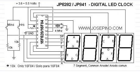
12Hr Led clock 4
Published:2013/1/10 21:55:00 Author:muriel | Keyword: 12Hr, Led clock

View full Circuit Diagram | Comments | Reading(582)
12Hr Led clock 3
Published:2013/1/10 21:54:00 Author:muriel | Keyword: 12Hr , Led clock

View full Circuit Diagram | Comments | Reading(559)
12Hr Led clock 2
Published:2013/1/10 21:53:00 Author:muriel | Keyword: 12Hr , Led clock
View full Circuit Diagram | Comments | Reading(2558)
12Hr Led clock
Published:2013/1/10 21:53:00 Author:muriel | Keyword: 12Hr, Led clock
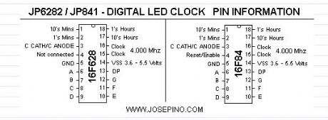
View full Circuit Diagram | Comments | Reading(774)
Minimum Mass Wireless LCD Display
Published:2013/1/10 21:51:00 Author:muriel | Keyword: Minimum Mass, Wireless , LCD Display
View full Circuit Diagram | Comments | Reading(1239)
LCD Display
Published:2013/1/10 21:50:00 Author:muriel | Keyword: LCD Display

View full Circuit Diagram | Comments | Reading(903)
LCD Clock/Calendar
Published:2013/1/10 21:49:00 Author:muriel | Keyword: LCD Clock/Calendar
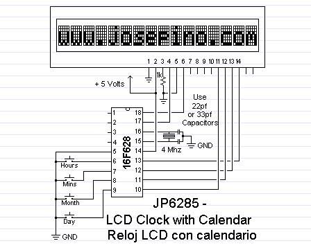
View full Circuit Diagram | Comments | Reading(837)
1.3W Power Amplifier
Published:2013/1/10 21:42:00 Author:muriel | Keyword: 1.3W, Power Amplifier

View full Circuit Diagram | Comments | Reading(944)
WIDE BAND ZERO CROSS DETECTORS
Published:2013/1/10 21:42:00 Author:muriel | Keyword: WIDE BAND, ZERO CROSS DETECTORS

View full Circuit Diagram | Comments | Reading(1856)
| Pages:205/2234 At 20201202203204205206207208209210211212213214215216217218219220Under 20 |
Circuit Categories
power supply circuit
Amplifier Circuit
Basic Circuit
LED and Light Circuit
Sensor Circuit
Signal Processing
Electrical Equipment Circuit
Control Circuit
Remote Control Circuit
A/D-D/A Converter Circuit
Audio Circuit
Measuring and Test Circuit
Communication Circuit
Computer-Related Circuit
555 Circuit
Automotive Circuit
Repairing Circuit