
Circuit Diagram
Index 2112
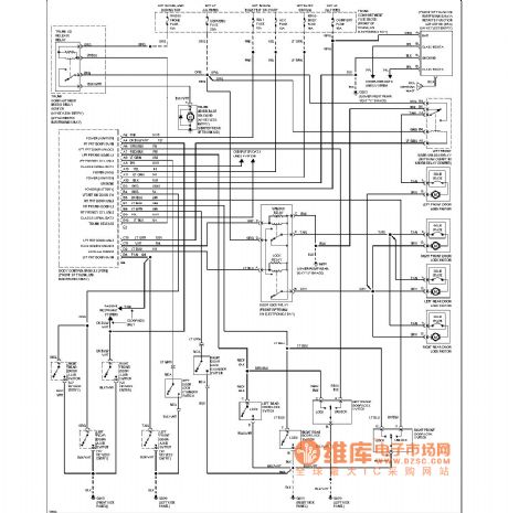
Cadillac electric door lock circuit
Published:2011/4/13 3:29:00 Author:Jessie | Keyword: electric door lock
View full Circuit Diagram | Comments | Reading(535)
Bridge type picked up horn protection circuit (2)
Published:2011/3/23 3:56:00 Author:Jessie | Keyword: horn protection

View full Circuit Diagram | Comments | Reading(534)
TOP232Y 3 road output switching supply circuit diagram
Published:2011/3/24 3:24:00 Author:Ecco | Keyword: output switching supply
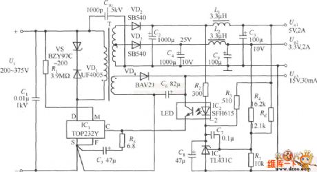
The TOP232 Y is used as four-terminal device. The efficiency of the power supply is 78%, the peak-crest value of output is 50 mv. Applied a single slab TOP232 Y, the total output of circuitry is 17.05 W. The d.c.inputs in the range of 200~375 V and 220 V/110 V. It needs to connect to rectifier filters, but no need to apply to input voltage doubler which make doubly rectification to 110 V voltage. The design develops soft start of TOP232 and undervoltage protection well, it has strict current limiting characteristic and high switch frequency characteristic, to make the magnetic core EE19 choosen by high - frequency transformer. Besides, TOP232 Y raises the spacing between the high pressure leak extreme and low-pressure port and lets up the electric leakage of pins, therefore power supply can used under worse environment. C1 is a type of d.c high frequency decoupling capacitance, and neglected when Ui is near from waiting source. The measuring resistance R1 could apply in settling the value of voltage UUV. When Rl=3.9MΩ, UUv=IUVRl=50μA×3.9MΩ=195V. When Ui<195 V, the supply will be cut off automaticly until Ui>195V. (View)
View full Circuit Diagram | Comments | Reading(1517)
DMAl0 Rectifier module structure chart
Published:2011/3/21 2:07:00 Author:muriel | Keyword: DMAl0, Rectifier module structure chart
View full Circuit Diagram | Comments | Reading(634)
CW494 Double-pointed convertor switching regulated power supply circuit diagram
Published:2011/3/27 20:30:00 Author:Ecco | Keyword: Double-pointed convertor , regulated power supply

The circuit diagram CW494 is a type of modulator integrated circuit made from of double-pointed convertor, including an error amplifier, reference voltage source, clock oscillator and vein breadth modulator,etc. The transformer T1 is a high - frequency transformer, which can deliver the energy to the burden. The T2 is a type of driving push transformer, which can deliver the two energizing pulses put by CW494 pulse modulator and amplifiered by energizing drive transistor. And the pulses reach the drive and base of switching tube in push-pull converter circuit diagram. After the variation of voltage and rectification of the pulses from samlping resistance by voltage transformer. The samlping resistance sends the pulses to the pulse modulator circuit diagram CW494, and to be the inverting input of error amplifier. Moreover, the switching power tube adopts rapid series F461. In the places of the feedback fo voltage , the input and output are connected directly. When the input, output need to be insulated, it can adopt photocoupler.
(View)
View full Circuit Diagram | Comments | Reading(905)
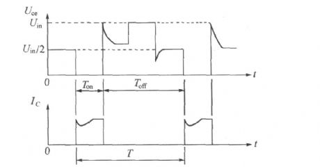
DMAl0 Double half bridge translation circuit principle diagram
Published:2011/3/21 2:11:00 Author:muriel | Keyword: DMAl0, Double half bridge , translation circuit, principle diagram
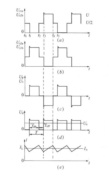
DMAl0 Main circuit work waveform:
(View)
View full Circuit Diagram | Comments | Reading(714)
ZP200(400)II Monitoring alarm interface circuit
Published:2011/3/23 2:15:00 Author:muriel | Keyword: ZP200(400)II, Monitoring alarm , interface circuit
View full Circuit Diagram | Comments | Reading(381)
Light modulator receive circuit diagram
Published:2011/3/24 2:46:00 Author:Ecco | Keyword: Light modulator receive

Q1, Q2 constitute of two class transistor amplifiers and used as zooming the modulating output semaphore of silicon solar battery. To 5lm/ft2 (lft=30.48 cms) beam of light modulated by 1000HZ, when the R is requlated to the biggest gain, the circuitry will produce 1V virtual value of voltage in output port.
Thiscircuitry issuitable foroptics correspondence andwarning system. (View)
View full Circuit Diagram | Comments | Reading(598)
The circuit diagram of electric energy meter with ADE7752
Published:2011/3/24 3:43:00 Author:Ecco | Keyword: electric energy meter

The circuit diagram of electric energy meter with ADE7752: (View)
View full Circuit Diagram | Comments | Reading(3207)
Boost type power fator correction electrical schematic
Published:2011/3/23 2:23:00 Author:muriel | Keyword: Boost type , power fator correction, electrical schematic
View full Circuit Diagram | Comments | Reading(415)
13.8V switching (voltage) regulator supply circuit diagram
Published:2011/3/20 22:47:00 Author:Ecco | Keyword: SI81206Z, 13.8V supply, switching (voltage) regulator
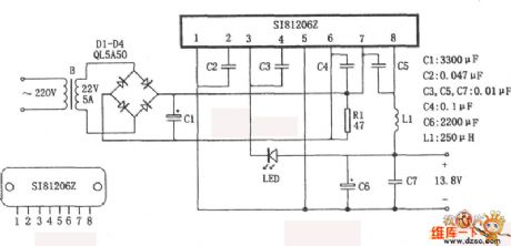
The 13.8 V switching (voltage) regulator supply is composed of SI81206 Z mold mass. The 13.8 V's power supply is used as a base station, car to carry an isoelectronic instrument. It has the features of high efficient, simple structure, steady performance.etc. (View)
View full Circuit Diagram | Comments | Reading(1824)
Half bridge converter electrical schematic diagram
Published:2011/3/21 2:15:00 Author:muriel | Keyword: Half bridge, converter , electrical schematic diagram
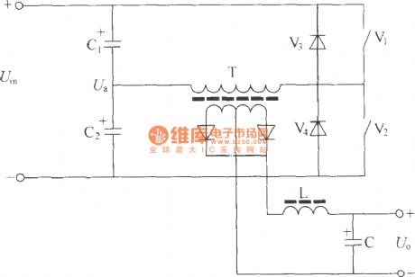
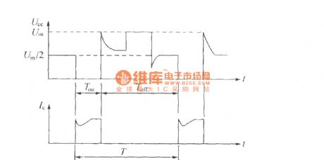
Half bridge converter typicalwaveform:
(View)
View full Circuit Diagram | Comments | Reading(965)
DC motor speed control circuit
Published:2011/3/23 3:32:00 Author:Jessie | Keyword: DC motor, speed control

This circuit can be used to control the rotating speed and direction of low power dc motors, series motorsor parallel motors. Motorsseries with rectifier bridge G1, then access them to the power transformer secondary windings n2. If rectifier bridge output terminal is impassability, motor stops, this is like potentiator's sliding contacts RP inmiddle position, if sliding contacts move upward or downward, then motor will rotate positive direction or reverse direction, so it can control the rotating of motor.
(View)
View full Circuit Diagram | Comments | Reading(667)
Thermistors protection rectifier circuit
Published:2011/3/23 3:55:00 Author:Jessie | Keyword: Thermistors, protection, rectifier
View full Circuit Diagram | Comments | Reading(392)
Full-Bridge converter electrical schematic diagram
Published:2011/3/21 2:26:00 Author:muriel | Keyword: Full-Bridge converter , electrical schematic diagram
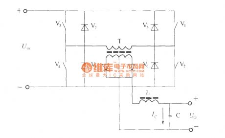
Full-Bridge converter typical waveform:
(View)
View full Circuit Diagram | Comments | Reading(737)
Positive voltage reference circuit
Published:2011/4/13 2:32:00 Author:may | Keyword: Positive voltage reference

View full Circuit Diagram | Comments | Reading(930)
PLL pulse generator(74HC4060、TC9122P)
Published:2011/4/13 2:38:00 Author:Ecco | Keyword: PLL , pulse generator

The PLL pulse generator is shown as the chart. The circuit is the phase-locked loop (PLL) pulse generator circuit. PLL makes a fractional frequency to crystal oscillator and gets 1kHz stepped frequency signal, moreover, it obtains 10kHz 999kHz pulse waveform on the output terminal. The manifold block 74HC4060 is a type of integrated chip with NOT gate and 1/2n frequency dividing circuit inside, among them, the NOT gate and the crystal oscillator with 4.096MHz form a oscillator circuit, and the frequency dividing circuit gets lkHz reference frequency signal by it.TC9122P is a high-speed programmable counter and its dividing ratio is decided by the BCD code, the programming data make the frequency ratio range be in 8 to 999, the circuit operates under the dividing ratio between 10 and 999. There are 3 types of phase comparator in 74HC4060, and the phase comparator PC2 can compare the output frequency with the positive edge of reference frequency, and get their feedback. The oscillation frequency of VC0 is decided by Cx, R1 and R2.
(View)
View full Circuit Diagram | Comments | Reading(5581)
Negative voltage reference circuit 2
Published:2011/4/13 2:31:00 Author:may | Keyword: Negative voltage reference

View full Circuit Diagram | Comments | Reading(857)
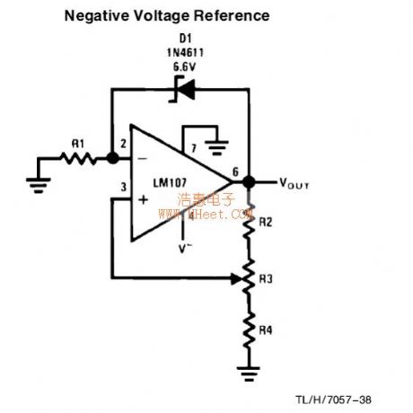
Negative voltage reference circuit
Published:2011/4/13 2:30:00 Author:may | Keyword: Negative voltage reference
View full Circuit Diagram | Comments | Reading(1101)
50Hz/1000W Inverterd power supply diagram with DC/AC IPM module
Published:2011/3/23 21:22:00 Author:muriel | Keyword: 50Hz/1000W, Inverterd power supply diagram , DC/AC IPM module
View full Circuit Diagram | Comments | Reading(1616)
| Pages:2112/2234 At 2021012102210321042105210621072108210921102111211221132114211521162117211821192120Under 20 |
Circuit Categories
power supply circuit
Amplifier Circuit
Basic Circuit
LED and Light Circuit
Sensor Circuit
Signal Processing
Electrical Equipment Circuit
Control Circuit
Remote Control Circuit
A/D-D/A Converter Circuit
Audio Circuit
Measuring and Test Circuit
Communication Circuit
Computer-Related Circuit
555 Circuit
Automotive Circuit
Repairing Circuit