
Circuit Diagram
Index 2049
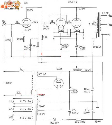
2A3 A class single-ended electron tube parallel amplifier circuit diagram
Published:2011/4/2 4:34:00 Author:Nicole | Keyword: electron tube
View full Circuit Diagram | Comments | Reading(5082)
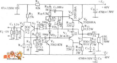
The power amplifier circuit diagram based on OCL
Published:2011/4/2 4:28:00 Author:Nicole | Keyword: power amplifier
View full Circuit Diagram | Comments | Reading(1836)
High-power electron tube single-ended A class 845 amplification circuit diagram
Published:2011/4/20 9:09:00 Author:Nicole | Keyword: electron tube

View full Circuit Diagram | Comments | Reading(2955)
Bridge exporting audio power amplification circuit diagram composed of two amplifiers in lm4752
Published:2011/4/20 9:08:00 Author:Nicole | Keyword: amplifier, audio power amplification

View full Circuit Diagram | Comments | Reading(1682)
Single-ended forward converter circuit diagram
Published:2011/3/30 3:28:00 Author:Nicole | Keyword: converter
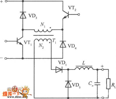
The figure is a single-ended forward converter circuit composed of two transistors, diode clamped. VTl and VT2 is on/offsimultaneously by PWM pulse excitation. When they off, the voltage on N1 is polarity reversed, diodes VD3 and VD4 on, the potentialis clamped. Therefore, the voltage which is added to collector is equal to the input voltage Ui during the VTl, VT2 off.
(View)
View full Circuit Diagram | Comments | Reading(866)
Single-ended flyback switching power supply circuit diagram
Published:2011/4/1 3:50:00 Author:Nicole | Keyword: single-ended switching power supply

View full Circuit Diagram | Comments | Reading(744)
Protecting circuit diagram of ring switch on
Published:2011/4/1 3:51:00 Author:Nicole | Keyword: ring switch

View full Circuit Diagram | Comments | Reading(683)
Condenser microphone(microphone)internal preamplifier circuit diagram
Published:2011/4/1 3:50:00 Author:Nicole | Keyword: Condenser microphone, microphone

View full Circuit Diagram | Comments | Reading(4439)
TA7642 integrated circuit radio circuit diagram
Published:2011/4/1 3:57:00 Author:Nicole | Keyword: integrated circuit, radio

View full Circuit Diagram | Comments | Reading(7139)
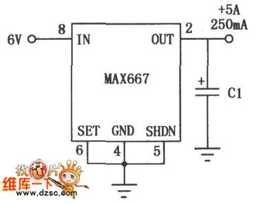
Application circuit diagram of MAX667 multifunction linear integrated regulator with high-precision
Published:2011/4/1 3:57:00 Author:Nicole | Keyword: linear integrated regulator
View full Circuit Diagram | Comments | Reading(539)
MAX639 series multi-function integrated switching regulator circuit diagram of fixed / adjustable output
Published:2011/4/1 3:58:00 Author:Nicole | Keyword: integrated switching regulator

MAX639 series fixed / adjustable output multi-function integrated switching regulator circuit is an efficient, multi-function switching regulator circuit, the output voltage is +5 v, the input voltage is 5.5 ~ 11.5V, output current is 100mA. It is efficient, the electronic switch control terminal of the logic level control and the battery-side low-voltage detectionare havethe advantages of low-power, low dropout, multi-functional, it is widely used in portable instruments, meters and so on. The basic application as shown. The typical application circuit of voltage detection can be see as below.
(View)
View full Circuit Diagram | Comments | Reading(1717)
Application circuit diagram of switching regulator with input l0 ~ 15V / Output 5V/3A
Published:2011/4/1 3:32:00 Author:Nicole | Keyword: switching regulator

View full Circuit Diagram | Comments | Reading(874)
Application circuit diagram of output voltage circuit can be connected into two kinds
Published:2011/4/1 3:31:00 Author:Nicole | Keyword: output voltage circuit
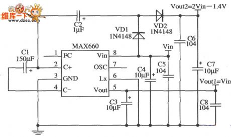
MAX660 can be connected into two kinds of output voltage circuit: Voutl=Vin;Vout2=2Vin-1.4 V. Output resistance of this circuit is slightly larger, as shown.
(View)
View full Circuit Diagram | Comments | Reading(572)
Fore input power supply circuit diagram using depressurization switching power supply
Published:2011/4/20 9:05:00 Author:Nicole | Keyword: switching power supply

View full Circuit Diagram | Comments | Reading(887)
74 series digital circuit of 74107 74LSO7A double J - K edge trigger
Published:2011/4/2 3:56:00 Author:Ecco | Keyword: digital circuit, double J - K negative edge, trigger

74 series digital circuit of 74107 74LSO7A double J - K negative edge trigger( with remove terminal)
(View)
View full Circuit Diagram | Comments | Reading(1558)
74 series digital circuit of 74LS113 74S113 double J - K negative edge trigger
Published:2011/3/31 21:18:00 Author:Ecco | Keyword: digital circuit , double J - K , negative edge trigger

74 series digital circuit of 74LS113,74S113 double J - K negative edge trigger (with preset)
(View)
View full Circuit Diagram | Comments | Reading(1235)
74 series digital circuit of 74116 dual 4-bit latch
Published:2011/4/2 3:55:00 Author:Ecco | Keyword: digital circuit , dual 4-bit latch


View full Circuit Diagram | Comments | Reading(852)
74 series digital circuit of 74120 pulse synchronizer/driver
Published:2011/4/2 3:55:00 Author:Ecco | Keyword: digital circuit, pulse synchronizer, pulse driver

74120 double pulse synchronizer/driver
It producesa single or a series of synchronous pulse with controlling function; Latch job promises that the output pulse won't be cut wave. High fan-outoutput complementary connects clock line drive system.
(View)
View full Circuit Diagram | Comments | Reading(702)
Dual D flip-flop VCO
Published:2011/4/18 20:14:00 Author:Ecco | Keyword: Dual D, flip-flop , VCO
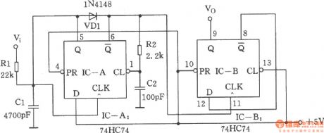
The chart shows the dual D flip-flop VCO. Circuit outputs a 50% duty cycle square wave signal, while the consumption of current is very low. When the input voltage is 5 ~ 12V, the output frequency ranges from 20 ~ 70kHz. First assuming the initial state of IC-A is Q = low level. At this time, VDl turns off, Vi charges to Cl through Rl. When the voltage on Cl reaches a certain voltage level, IC-A is forced to flip, its Q output is in high level, Cl discharges through VDl. At the same time, the CL input of IC-A will be transformed into low level, IC-A is forced back to Q = low level. The delay effect of R2 and C2 discharges the electricity of C1 before the IC-A returning to the state of Q = low level. The narrow pulse current of IC-A triggers IC-B, it produces a 50% duty cycle output pulse signal.
(View)
View full Circuit Diagram | Comments | Reading(1496)
4h Timing circuit composed of 556
Published:2011/4/14 3:42:00 Author:Ecco | Keyword: 4h , Timing circuit

The figure shows 4h timing circuit which is composed of 556 dual time base circuit. To access N8281 divider network in the middle of 556 dual time base circuit, it will get a long time delay without large volume of capacitors. The first l / 2 (556) works in the way of oscillator, the period is l / f. It will produce the signal output in a N / f cycle to trigger the other half 1 / 2 (556) to add the output of oscillator to N divider network. It decides the total delay produced by the dividerto connect the divider to ⑧ pin of the second 1 / 2 (556) input terminal. Delay time is divided in 4 blocks of 30min, 1h, 2h, 4h. If connecting N8281 crossover in series additionally , the total amount of delay can be increased to days or even weeks.
(View)
View full Circuit Diagram | Comments | Reading(1783)
| Pages:2049/2234 At 2020412042204320442045204620472048204920502051205220532054205520562057205820592060Under 20 |
Circuit Categories
power supply circuit
Amplifier Circuit
Basic Circuit
LED and Light Circuit
Sensor Circuit
Signal Processing
Electrical Equipment Circuit
Control Circuit
Remote Control Circuit
A/D-D/A Converter Circuit
Audio Circuit
Measuring and Test Circuit
Communication Circuit
Computer-Related Circuit
555 Circuit
Automotive Circuit
Repairing Circuit