
Index 239
PRECISION_FREQUENCY_COUNTER_TACHOMETER
Published:2009/7/7 23:16:00 Author:May

In this configuration, the display reads hertz directly. With pin 11 of the ICM7027A connected to VDD, the gating time will be 0.1 second; this will display tens of hertz as the least significant digit. For shorter gating times, an ICM7207 can be used with a 6.5536-MHz crystal, giving a 0.01 second gating with pin 11 connected to VDD, and a 0.1 second gating with pin 11 open. (View)
View full Circuit Diagram | Comments | Reading(1571)
STUD_FINDER
Published:2009/7/7 23:15:00 Author:May


The CS209 is designed to detect the presence or proximity of magnetic metals. It has an internal oscillator that, along with its extemal lc resonant circuit, provides oscillations whose amplitude is dependent upon the Q of the lc network. Close proximity to magnetic material reduces the Q of the tuned circuit, thus the oscillations tend to decrease in amplitude. The decrease in amplitude is detected and used in tum on LED1, indicating the presence of a magnetic material (i.e., nail or screw). (View)
View full Circuit Diagram | Comments | Reading(3067)
PAPER_SHEET_DISCRIMINATOR_FOR_PRINTING_AND_COPYING_MACHINES__
Published:2009/7/7 23:14:00 Author:May
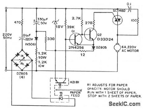
The circuit outputs power to the drive motor when one or no sheets are being fed, but interrupts motor power when two or more superimposed sheets pass through the optodetector slot. The optodetector can be either an H2aB darlington interruptor module or an H23B matched emitter-detector pair. The output from the optodarlington is coupled to a Schmitt trigger, comprising transistors Q1 and Q2 for noise immunity and minor paper opacity variation immunity. When the Schmitt is on, gate current is applied to the SC148D output device. The dc power supply for the detector and Schmitt is a simple rc diode halfwave configuration chosen for its low cost (fewer diodes and no transformers) and minimum bulk. While such a supply is directly coupled to the power triac, this is precluded by current drain considerations (50 mA dc for the gate drive alone). Note that direct coupling of the Schmitt to the output triacs is preferred, since RFI is virtually eliminated with the quasi-dc gate drive. (View)
View full Circuit Diagram | Comments | Reading(588)
PICOAMMETER_CIRCUIT
Published:2009/7/7 23:12:00 Author:May
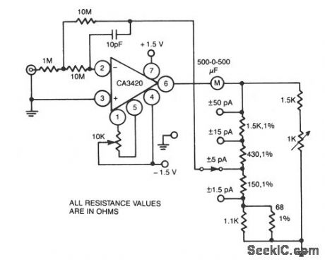
This circuit uses the exceptionally low input current 0.1 pA of the CA3420 BiMOS op amp. With only a single 10-MΩ resistor, the circuit covers the range from ± 50 pA to a maximum full-scale sensi-tivity of ±1.5 pA. (View)
View full Circuit Diagram | Comments | Reading(0)
BIPOLAR_ANALOG_TWO_QUADRANT
Published:2009/7/7 23:11:00 Author:May

Bipolar reference voltage for upper Precision Monolithics DAC-08 D/A converter modulates reference current by ±1.0 mA around quiescent current of 1.1 mA. Lower DAC-08 has same 1.1-mA reference current and effectively subtracts out quiescent 1.1 mA of upper reference current at all input codes since voltage across R3 varies between -10 V and 0 V. Output voltage E0 is thus product of digital input word and bipolar analog reference voltage.-J. Schoeff and D. Soderquist, Differential and Multiplying Digital to Analog Converter Applications, Precision Monolithics, Santa Clara, CA, 1976, AN-19, p 3. (View)
View full Circuit Diagram | Comments | Reading(1536)
QRP_SWR_BRIDGE
Published:2009/7/7 23:08:00 Author:May
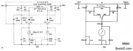
The design shown is a simple unit for QRP operation on all authorized frequencies up to 30 MHz, based on a toroidal transformer T1. The secondary winding of T1 samples a small amount of rf power, both forward and reflected, which is divided by the bridge circuit and rectified by diodes D1and D2. Forward and reflected readings are obtained simultaneously on the two meters Ml and M2, and the bridge is matched and balanced at the required load impedance by C1 and C2. See Fig. 56-9b for an alternative, less expensive, single meter version. The bridge also measure forward power. (View)
View full Circuit Diagram | Comments | Reading(1251)
VERY_SHORT_PULSE_WIDTH_MEASURER
Published:2009/7/7 23:06:00 Author:May
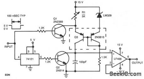
This circuit operates by charging a small capacitor from a constant-current source when the pulse to be measured is present. Dual pnp transistor Q3 is the current source; its output current equals the LM329 reference voltage divided by the resistance of potentiometer R1. When the input is high with no pulse present, Q1 keeps the current source turned off. When the pulse begins and the input decreases, Q1 turns off and the monostable multivibrator generates a short pulse. The pulse from the multivibrator turns on Q2, removing any residual charge from the 100-pF capacitor. Q2 then turns off, and the capacitor begins to charge linearly from the current source. When the input pulse ends, the current source turns off, and the voltage on the capacitor is proportional to the pulse width.
(View)
View full Circuit Diagram | Comments | Reading(620)
FOUR_QUADRANT_8_BIT
Published:2009/7/7 23:06:00 Author:May

Requires only three Precision Monolithics DAC-08D/A converters to provide high-speed multiplication of two 8-bit digital words and give analog output.-J Schoeff and D. Soderquist, Differential and Multiplying Digital to Analog Converter Applications, Precision Monolithics, Santa Clara.CA,1976,AN-19,p7. (View)
View full Circuit Diagram | Comments | Reading(591)
AC_COUPLED_MU_LTIPLICATION
Published:2009/7/7 23:02:00 Author:May
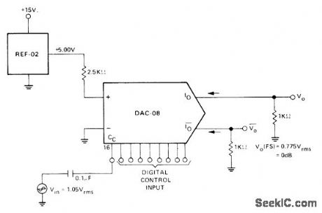
Combination of Precision Monolithics REF-02 voltage reference and DAC-08 DIA converter uses compensation capacitor terminal Cc as input. With full-scale input code, output Vo is flat to above 200 kHz and 3 dB down at 1 MHz, for multiplying applications far beyond audio range. Circuit has high input impedance, as often required to avoid loading high source impedance. Dynamic range is greater than 40 dB.-J. Schoeff and D. Soderquist, Differential and Multiplying Digital to Analog Converter Applications, Precision Monolithics, Santa Clara, CA, 1976, AN-19, p 4. (View)
View full Circuit Diagram | Comments | Reading(1330)
_OUTPUT_LEVEL_SHIFTER
Published:2009/7/7 22:58:00 Author:May

Transistors connected to Motorola MC1595L linear four-quadrant multiplier perform level shifting for applications requiring output having ground reference. Temperature sensitivity of circuit is minimized by using complementary transistors in same package, such as MD6100, in place of upper two transistors. If high output impedance and low current drive are drawbacks, opamp can be connected as source-follower output stage.-E. Renschler, Analysis and Basic 0peration of the MC1595, Motorola, Phoenix, AZ, 1975, AN-489, p 10. (View)
View full Circuit Diagram | Comments | Reading(1482)
FOUR_QUADRANT
Published:2009/7/7 22:53:00 Author:May
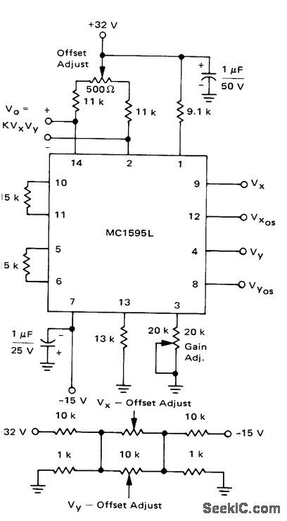
Motorola MC1595L linear four-quadrant multiplier takes two different input voltages, each between -10V and +10V, and gives output equal to one-tenth of their product. Circuit can be operated in either AC or DC mode. Design and setup procedures are given.-E. Renschler, Analysis and Basic Operation of the MC1595, Motorola, Phoenix, AZ, 1975, AN-489 p 8. (View)
View full Circuit Diagram | Comments | Reading(720)
ANALOG_MULTIPLIER
Published:2009/7/7 22:51:00 Author:May

Multiplier and amplifier sections of Exar XR-S200 PLL IC are combined to perform analog multiplication without need for DC level shifting between input and output. Single-ended output is at ground level. - Phase-Locked Loop Data Book, Exar Integrated Systems, Sunnyvale, CA, 1978, p 9-16. (View)
View full Circuit Diagram | Comments | Reading(0)
WIRELESS_TELEPHONE_EAVESDROPPER
Published:2009/7/7 22:49:00 Author:May
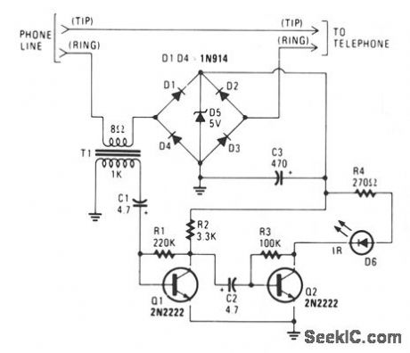
The IR transmitter connects to a telephone circuit, and transmits both sides of all telephone conversations to any line-of-sight location, within 40 feet. No power is taken from the central office, as long as all phones remain on-hook. The current flows through the phone and back to the central offtce, thereby keying their equipment. We tap into the telephone line by connecting the IR transmitter circuit in series with either the tip or ring. When the telephone is off-hook, current will flow through the diode bridge polarity protector and supply the power for the IR transmitter. The phone's audio information is taken off the line by transformer T1. The 1000-Ω winding of the transformer connects to a two-stage transistor audio amplifier/modulator. A 2000-Ω potentiometer could be added to the input of the two-stage amplifter to control the modulation level, and another potentiometer could be added in place of R3 to adjust the IR's idle current. (View)
View full Circuit Diagram | Comments | Reading(876)
APPROXIMATING_VECTOR_SUMS
Published:2009/7/7 22:48:00 Author:May

Combination of two opamps and Analog Devices 433 multiplier1divider IC provides output voltage equal to vector sum of two input voltages, by computing square root of sum of squares.-D.H. Sheingold, Approximate Analog Functions with a Low-Cost Multiplier/Divider, EDN Magazine, Feb. 5, 1973, p 50-52. (View)
View full Circuit Diagram | Comments | Reading(645)
FOUR_QUADRANT_WITHOUT_LEVEL_SHIFT
Published:2009/7/7 22:45:00 Author:May
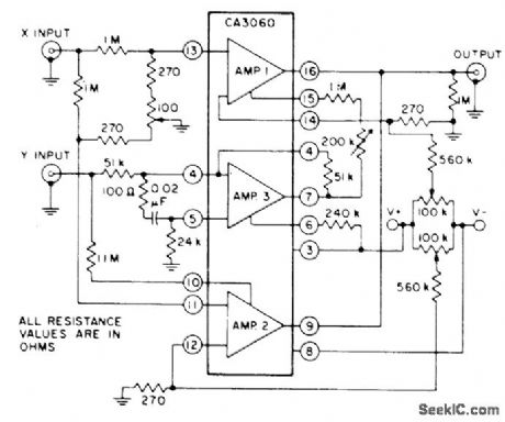
CA3060 three-opamp array provides four-quad-rant multiplication without level shift between input and output. Circuit includes adjustments associated with differential input and adjustment for equalizing gains of amplifiers 1 and 2.Amplifier 3 is connected as unity-gain inverter- Linear Integrated Circuits and M0S/FET's, RCA Solid State Division, Somerville, NJ, 1977, p 153. (View)
View full Circuit Diagram | Comments | Reading(633)
TWO_QUADRANT
Published:2009/7/7 22:39:00 Author:May

Bipolar digital multiplier has output polarity controlled by offset-binary-coded digital input word. Precision Monolithics DAC-08 D/A converter drives OP-02 opamp. 0utput is symmetrical about ground.-J. Schoeff and D. Soderquist, Differential and Multiplying Digital to Analog Converter Applications, Precision Monolithics, Santa Clara, CA, 1976, AN-19,p2. (View)
View full Circuit Diagram | Comments | Reading(2600)
APPROXIMATING_COSINES
Published:2009/7/7 22:34:00 Author:May

Analog Devices 433 multiplier/divider IC approximates cosine of angle to better than 1%, by computing nonintegral exponents. 0nly one opamp is needed. Approximation uses arbitrary exponent as one term of cosineθplus a linear term and a constant term, as described in article.-D. H. Sheingold, Approximate Analog Functions with a Low-Cost Multiplier/Divider, EDN Magazine, Feb. 5, 1973, p 50-52. (View)
View full Circuit Diagram | Comments | Reading(687)
CASSETTE_INTERFACE
Published:2009/7/7 22:32:00 Author:May
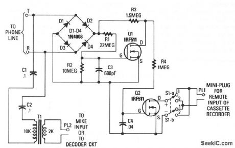
Q1 and Q2 are used to form the basis of an interface circuit for attaching a cassette recorder to the phone line. The circuit does not require a power supply because operating power is drawn from the telephone line itself. The incoming signal is fed across a bridge-rectifier circuit, consisting of diodes D1 through D4.When the phone is on hook, the voltage at the output of the bridge at the R1/R3 junction is near 48 V.That voltage is fed across a voltage divider consisting of R1 and R2. The voltage at the junction formed by R1 and R2 is fed to the gate of Q1, turning it on. That pulls the drain of Q1 low. Since the gate of Q2 is connected to the drain of Q1, the bias applied to the gate of Q2 is low, holding it in the OFF state.When the answering machine responds to a call or a phone is taken off hook, the voltage across the phone lines drops below 10 V, causing Q1 to turn off. At that point, the voltage at Q1's drain rises, turning Q2 on. The remote input of the cassette is connected to Q2's drain and source through S1, and a miniature plug is connected to the remote input jack.Switch S1 must be in a position so that the positive lead of the recorder's remote input connects, through switch position 1, to Q2's drain and the negative input to Q2's source. Switch S1 provides a convenient way to reverse the circuit's trigger output without having to unsolder and resolder leads. The phone's audio is coupled through C1, C2, and T1 to the microphone input of the cassette recorder. (View)
View full Circuit Diagram | Comments | Reading(2452)
STEREO_POWER_METER
Published:2009/7/7 22:32:00 Author:May
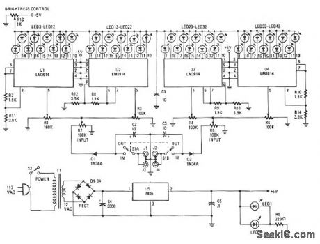
The Stereo Power Meter is made up of two identical circuits and a power supply. Each circuit contains two LM3914 display chips which contain 10 voltage comparators, a 10-step voltage divider, a referencevoltage source, and a mode-select circuit that selects a bar or dot display via a logic input at pin 9. The brightness of the LEDs is controlled by the 1900-Ω resistors and the reference voltage is controlled by the 3900-Ω resistors. The 10-step voltage divider within the chips is connected between the reference voltage and ground. Since each step of the voltage divider is separated by a 1-KΩ resistor, each comparator senses voltage 10% greater than the preceding comparator. The signal is applied to pin 5, which is buffered through a resistor-diode network and then amplified as it passes to each of the10 comparators. Each LED is arounded through the comparators as the input signal voltage matches the reference voltage. That results in one to 10 LEDs illuminating as the signal voltage increases. (View)
View full Circuit Diagram | Comments | Reading(1857)
3_IN_1_TEST_SET
Published:2009/7/7 22:30:00 Author:May

This circuit is designed around a 4049 hex inverter/buffer. Two inverters are used in a dual-frequency signal-injector circuit, another inverter is used as a logic probe, and the remaining three inverters are used as a sensitive dual-input, audio-signal tracer.The signal-injector potion gates are configured as a two-frequency, pulse-generator circuit. Under normal conditions, the generator's output frequency is around 10 kHz, but when S2 is closed, the output frequency drops to about 100 Hz. The logic-probe potion is made up of U1c, the output of the inverter decreases. The low output of U1c reverse biases LED2, so it remains off. That low output also forward biases LED1, causing it to light. But when a logic low presented Ulc's input, the situation is reversed, so LED2 lights and LED1 darkens.The audio-signal tracer portion is made up of the three remaining inverters which are configured as a linear audio amplifier to increase the input signal level by a factor of 10 or 100. The amplified output signal feeds a miniature piezo element of audible detection.
(View)
View full Circuit Diagram | Comments | Reading(1566)
| Pages:239/471 At 20221222223224225226227228229230231232233234235236237238239240Under 20 |
Circuit Categories
power supply circuit
Amplifier Circuit
Basic Circuit
LED and Light Circuit
Sensor Circuit
Signal Processing
Electrical Equipment Circuit
Control Circuit
Remote Control Circuit
A/D-D/A Converter Circuit
Audio Circuit
Measuring and Test Circuit
Communication Circuit
Computer-Related Circuit
555 Circuit
Automotive Circuit
Repairing Circuit