
Index 226
TRIAC_CONTROLLED_VOLTAGE_DOUBLER
Published:2009/7/9 3:11:00 Author:May
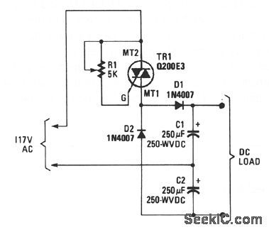
View full Circuit Diagram | Comments | Reading(713)
LOW_POWER_INVERTER
Published:2009/7/9 3:07:00 Author:May
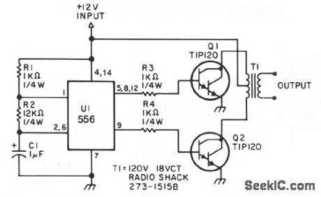
This low-power inverter uses only 9 parts and turns 10 to 16 Vdc into 60-Hz, 115-V square-wave powqr to operate ac equipment up to 25 W. The first section of the 556 timer chip is wired as an astable oscillator with R2 and C1 setting the frequency. The output is available at pin 5. The second section is wired as a phase inverter. That output is available at pin 9. Resistors R3 and R4 keep output trans;stors Q1 and Q2 from loading down the oscillator. The two transistors drive the transformer push-pull fashion.When one transistor is biased-on, the other is cut-off. The transformer is a 120 V/18 VCT unit that is connected backwards, so that it steps the voltage up rather than down. Oscillator circuit U1, R1, R2, and C1 operates from about 4 to 16 V with a very stable output. (View)
View full Circuit Diagram | Comments | Reading(742)
ELECTRONIC_LEVEL
Published:2009/7/9 2:52:00 Author:May


An electronic level can be constructed using two mercury switches mounted on an absolutely flatboard,along with the LEDs.If one LED lights,the surfaceis not level,If both light,the surface is level. (View)
View full Circuit Diagram | Comments | Reading(943)
FULL_BATHTUB_INDICATOR
Published:2009/7/9 2:52:00 Author:May
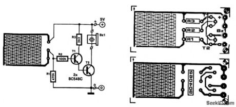
Running a bath can end in a minor domestic disaster if you forget to turn off the taps 'n time. This indicator activates an active buzzer to provide an audible warning when a given water level is reached.
Because the water sensor and the driver circuit for the buzzer are contained on one PC board, the indicator, together with the 9-V battery and the buzzer, can be built into a compact case. Obviously, the sensor, which is etched on the PC-board, must not be fitted in case-iron or steel bath, the indicator is secured to it with the aid of a magnet glued onto the case. To prevent scratching the bath, the magnet can be covered in plastic or rubber. If you have a polypropylene bath, the indicator can be stuck to it with blue tack or double-sided adhesive tape.
When the water reaches the sensor, the base of T1 is connected to the positive supply line. As a result, T1 and T2 are switched on so that the buzzer BZ1, a self-oscillating type, is activated. The current drawn by the circuit in that condition is about 25 mA.
In case the circuit is actuated by steam, its sensitivity can be reduced by increasing the value of R2. It is best to tin the PC board tracks to prevent corrosion.
T1, T2=BC548CBZ1 = active piezo-ceramic resonator (View)
View full Circuit Diagram | Comments | Reading(1920)
PREAMPLIFIER_FOR_MAGNETIC_PHONO_CARTRIDGES
Published:2009/7/9 2:49:00 Author:May

This amplifier is intended to be added to preamplifiers that have no phono input. Such a phono input is required for normal record players with a dynamic pick-up, of which millions are still around. Moreover, the amplifier does not only bring the output of the pick-up to line level, it also adds the correction to the fre-quency response (according to RIAA requirements).
When recording gramophone records, the frequency characteristic is lifted at the high end. This lift must be countered in the playback (pre)amplifier. The corrections to the frequency response characteris-tic are according to a norm set by the Record Industries Association of America (RIAA) and also by the IEC.
The corrective curve provided 'oy the amplifier is shown in the graph (bold line). The thin line shows the ideal corrective curve. The sharp bends in this at 50 and 500 Hz are nearly obtained in the practical curve by network R3lC2; just above 2 kHz is approached in practice by filter R5/R6/C3. The arrangement of R3/C2 in the feedback loop pf IC1 gives noticeably better results than the usual (passive) filter approach.
Circuit IC1 provides a dc amplification of 40 dB, which drops to about 20 dB when the frequency rises above 500 Hz. To minimize the (resistor) noise and the load of the op amp at higher frequencies, the value of R3 is a compromise. The associated polystyrene capacitor, CZ, should have a tolerance of 1 to 2%.
To raise the 2-mV output of the dynamic pick-up to line level at 1 kHz, linear amplifier IC2 has been added. This stage has a gain of 22 dB, so a signal of 250 mV is available at its output.
Capacitors C4/C5 at the output, in conjunction with the input impedance of the following preamplifier, form a high-pass filter with a cut-off frequency of 20 Hz; this serves to suppress any rumble or other low frequency noise. The value of C1 is normally given in the instruction booklet of the dynamic pick-up.
The power supply for the amplifier must be of good quality. Particularly, the transformer should be class Al with a small stray magnetic field.
When the amplifier is built into the record player (best), the power supply should not be included unless it is very well screened; otherwise, hum is unavoidable. (View)
View full Circuit Diagram | Comments | Reading(2484)
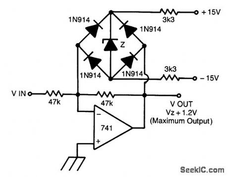
FAST_SYMMETRICAL_ZENER_CLIPPER
Published:2009/7/9 2:48:00 Author:May
The problem with using two zeners back to back in series to get symmetrical clamping is that the knee of the zener characteristics is rather sloppy. Also, charge storage in the zeners causes speed problems and the zeners will have slightly different knee voltages, so the symmetry will not be all that good. This circuit overcomes these problems.By putting the zener inside a diode bridge, the same zerxer voltage is always experienced. The voltage errors caused by the diodes are much smaller than those caused by the zener. Also, the charge storage of the bridge is much less. By biasing the zener ON all the time, the knee appears to be much sharper. (View)
View full Circuit Diagram | Comments | Reading(576)
PRECISION_FULL_WAVE_RECTFIER
Published:2009/7/9 2:45:00 Author:May
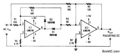
Using two op amps, this circuit produces a full-wave rectified version of the input signal. Op amp IC1 inverts the negative-going signal, but because of D2, it stays near zero. IC2 produces a positive-going sig-nal. For positive-going signals, IC1 produces a negative output through D1 to IC2, where it is combined with positive VIN from R4/R5. At the summing junction of IC2, the negative output of IC1 is doubled and inverted via IC2, R3, and R5 to produce + V0UT. This is summed with negative output of IC1 to produce + V0UT. (View)
View full Circuit Diagram | Comments | Reading(726)
DUAL_TRACKING_REGULATOR
Published:2009/7/9 2:45:00 Author:May
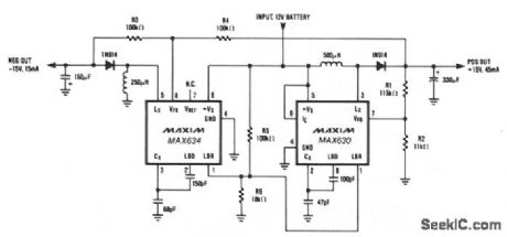
A MAX634 inverting regulator is combined with a MAX630 to provide a dual tracking ±5 output from a 12-V battery. The reference for the -15 V output is derived from the positive output via R3 and R4. Both regulators are set to maximize output power at low battery voltages by reducing the oscillator frequency, via LBR, when VBATT falls to 8.5V. (View)
View full Circuit Diagram | Comments | Reading(593)
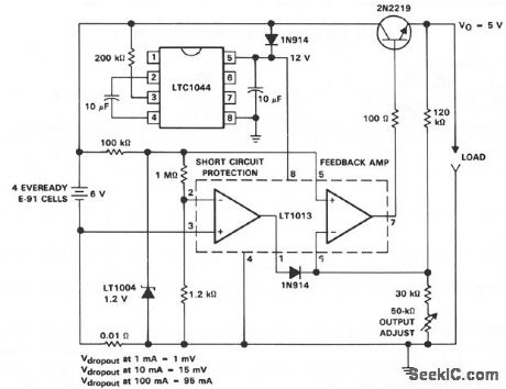
LOW_DROPOUT_5_V_REGULATOR
Published:2009/7/9 2:43:00 Author:May
View full Circuit Diagram | Comments | Reading(542)
VIDEO_DC_RESTORER
Published:2009/7/9 2:42:00 Author:May
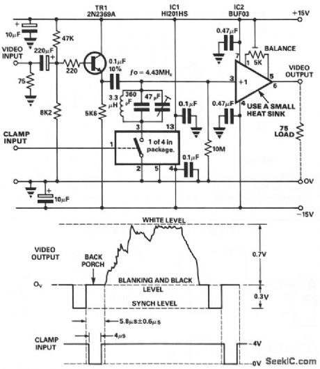
The main requirement for efficient dc restoration is to provide a short time-constant during the clamp period,with a long time-constant during the active line time.The switch within the Harris HI201HS has anon resistance of 30 Ω and the PMI buffer, BUF03,has an input resistance of 50 MΩ.The tuned circuit presents a high impedance at the 4.43-MHz color subcarrier frequency SO that the color-burst signal is retained if the video signal contains this information, (View)
View full Circuit Diagram | Comments | Reading(981)
PICTURE_FIXER_INVERTER
Published:2009/7/9 2:36:00 Author:May
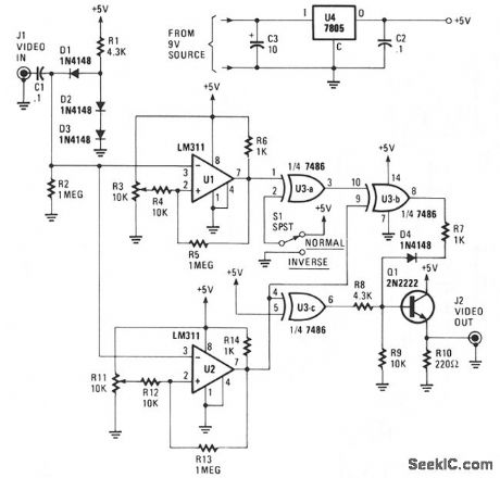
The circuit will accept a video signal, separate the sync pulses, invert the video, and add new video to the old sync pulses. The video signal is brought in through J1 and applied to a clamping circuit consisting of C1, D1, D2, D3, R1, and R2. The clamp circuit forces all of the sync pulses to align with the same dc voltage level. With the video voltage clamped, the trip points of the comparators that follow can be set with trimmer resistors R3 and R11. The resistors will not have to be readjusted. One comparator, U1, is adjusted to change states with a change in either video or sync-pulse levels. The other comparator, U2, is adjusted to trip on changes of sync-pulse levels only.The output of U1 now consists of a logic level, 0 to + 5 V, signal that contains both sync pulses and video. The composite signal is coupled to an EXCLUSIVE-OR gate, U3a, where it is either inverted or not inverted, depending upon the position of switch NORM/REV S1. The output, at pin 3 of U3a, is next sent to U3b. There the composite signal is combined with the sync-pulse only signal from U2. The EXCLUSIVE-OR action of U3b cancels out the sync pulses, leaving only video at the IC's output.Since the sync pulses are inverted as they pass through U2, they must be inverted once more before being combined with the video signal. That final inversion is performed by U3c, and that device's output is combined with that of U3b via D4, R7, R8, and R9. The newly combined signal is buffered by emitter-follower Q1, and sent to the outside world via J2. The circuit can be powered by a 9- to 12-V wall-mount power supply. The supply voltage is regulated down to 5 V by U4. (View)
View full Circuit Diagram | Comments | Reading(789)
BULL_HORN
Published:2009/7/9 2:36:00 Author:May
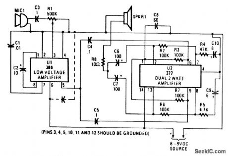
This bull horn uses U1 as a driver stage and U2 as an output driver. U1 is set up for a gain of 200. The microphone should have about 200-mVpp output. The two sections of U2 produce about 4-W of output power. Use shielded cable for all audio leads. Power is a 6-to 9-V battery or other source. (View)
View full Circuit Diagram | Comments | Reading(1298)
VOLTAGE_DOUBLER
Published:2009/7/9 2:32:00 Author:May

This circuit drives relays of 24 and 18 Vdc from a 12-V power supply. Use this circuit with almost any pnp or npn power transistor.Parts: U1: NE 555 timer. C1 and C2: 50 μF/ 25 Vdc. Q1: TIP 29, TIP120, 2N4922, TIP61, TIP110, or 2N4921. Q2: TIP30, TIP125, 2N4919, TIP62, TIP115, or 2N4918. (View)
View full Circuit Diagram | Comments | Reading(1466)
VIDEO_PALETTE
Published:2009/7/9 2:31:00 Author:May
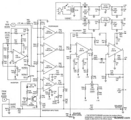
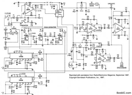
This system consists of two parts. The main board dissects the video signal and provides independent level control for burst, chroma, luminance, and sync signals, as well as phase and polarity. The video signal is reassembled in the output in corrected or modified format as required by the user. The effects board produces luminance inversion or can generate discrete luminance steps (posterization) or a nonlinear gray scale (solarization) to achieve simulation of photographic effects commonly seen in various special-effect photographic processes. The kit is available from North Country Radio, P.0. Box 53, Wykagyl Station, NY 10804. (View)
View full Circuit Diagram | Comments | Reading(1858)
VARIABLE_VOLTAGE_REFERENCE_SOURCE
Published:2009/7/9 2:30:00 Author:May
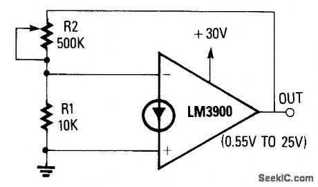


The noninverting terminal of the op amp is grounded, and the circuit uses the voltage at the inverting terminal as a reference. Its voltage gain is determined by the R2/R1ratio. When R2 is set at zero, the circuit has unity gain and a 0.55-V output. When R2 is set to the maximum value, the circuit has a gain of 50 and an output of about 25 V. The circuit provides good regulation and can supply output currents of several milliamps. The output voltage however, is not temperature compensated. (View)
View full Circuit Diagram | Comments | Reading(748)
LOW_COST_LOW_DROPOUT_LINEAR_REGULATOR
Published:2009/7/9 2:29:00 Author:May
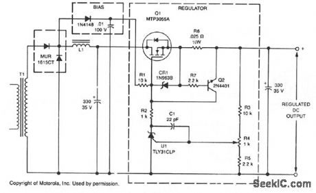
This linear post regulator provides 12 V at 3 A. It employs TL431 reference U1 which, without additional amplification, drives TMOS MTP3055A gate Q1 series pass regulator. Bias voltage is applied through R1 to Q1's gate, which is protected against overvoltage by diode CR1. Frequency compensation for closed-loop stability is provided by C1.Key performance features are: Dropout voltage: 0.6 V Load regulation: 10 mV Line regulation:±5 mV Output ripple: 10 mV pk-pk (View)
View full Circuit Diagram | Comments | Reading(2250)
PROGRAMMABLE_IDENTIFIER
Published:2009/7/9 2:24:00 Author:May

Used on an amateur or experimental radio beacon,the above ID circuit will generate any callsign or message programmed into the EPROM. A CD4020 CMOS counter is driven by an RC clock circuit.This addresses the EPROM.and serial data is available at pin 9. (View)
View full Circuit Diagram | Comments | Reading(1995)
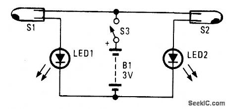
MULTIVIBRATOR_WITHLEDS
Published:2009/7/9 2:15:00 Author:May
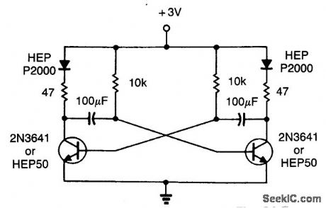
A simple astable multivibrator IS used to alternately flash two LEDs.The approximate time constant is 0.69.
(R1C1+R2C2) R1=R2=10 kΩ C1=C2=100μF (View)
View full Circuit Diagram | Comments | Reading(698)
PHASE_SELECTOR_PHASE_DETECTOR_SYNCHRONOUS_RECTIFIER_BALANCED_MODULATOR
Published:2009/7/9 2:12:00 Author:May


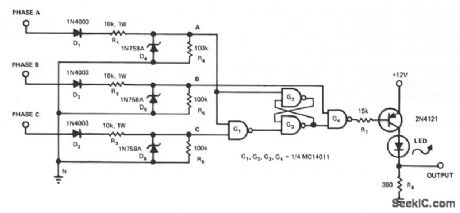
This circuit passes the input signal at unity gain, either unchanged or inverted, depending on the digital control input. A buffered input is shown, since low-source impedance is essential. Gain can be added by modifications to the feedback networks. Signals up to 100 kHz can be handled with 20.0-V pk-pk, output.The circuit becomes a phase detector when driving the digital control input with a reference phase at the same frequency as the input signal; the average dc output is proportional to the phase difference, with 0 V at +90°. By connecting the output to a comparator, which in turn drives the digital control, a synchronous full-wave rectifier is formed. With a low-frequency input signal and a high-frequency digital control signal, a balanced (suppressed carrier) modulator is formed. (View)
View full Circuit Diagram | Comments | Reading(1263)
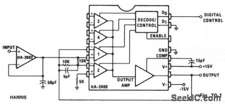
COMPOSITE_VIDEO_SIGNAL_TEXT_ADDER
Published:2009/7/9 2:11:00 Author:May
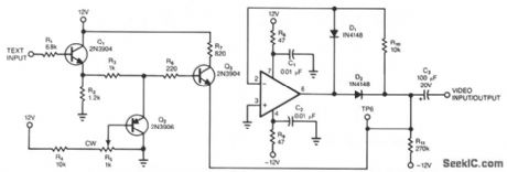
This circuit shows a simple way to add text information to a composite-video signal that might be floating at some indeterminate dc level. The text generator and composite-video source must have the same sync signal. The video-input and -output signals share the same terminal. C3 couples the video signal to the output of a rectifier circuit that is based on a subvideo-speed op amp. A faster op amp would clamp on individual sync pulses rather than on the video waveform's average value, as is desired. R11 serves as a pulldown resistor and feedback resistor R10 ensures that TP6 remains at ground level. Emitter follower Q1 buffers the text signal, and R5 serves as a gain control. A simple clamp circuit, Q2, is sufficient for regulating amplitude, because the text signal contains no gray-scale levels. Q3 couples the text signal into the op-amp clamp circuit. (View)
View full Circuit Diagram | Comments | Reading(1378)
| Pages:226/471 At 20221222223224225226227228229230231232233234235236237238239240Under 20 |
Circuit Categories
power supply circuit
Amplifier Circuit
Basic Circuit
LED and Light Circuit
Sensor Circuit
Signal Processing
Electrical Equipment Circuit
Control Circuit
Remote Control Circuit
A/D-D/A Converter Circuit
Audio Circuit
Measuring and Test Circuit
Communication Circuit
Computer-Related Circuit
555 Circuit
Automotive Circuit
Repairing Circuit