
Index 441
The photoelectric logic circuit diagram
Published:2011/3/30 22:16:00 Author:Ecco | Keyword: photoelectric logic

When Q1, Q2 phototransistors taking about 1075.4 IX(100 feet one candle) illumination, the output of Q3 is 0. When one or two phototransistorshave no or little illumination, the output of Q3 is positive or 1.
(View)
View full Circuit Diagram | Comments | Reading(426)
The inside circuit diagram of crystal diode STTH6006TV1、STTH60L6TV、STTH6110TV1
Published:2011/4/1 1:32:00 Author:Ecco | Keyword: crystal diode
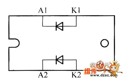
The inside circuit diagram of crystal diode STTH6006TV1、STTH60L6TV、STTH6110TV1 is as below:
(View)
View full Circuit Diagram | Comments | Reading(457)
The interface circuit diagram between MT8880 and SCM
Published:2011/3/30 22:10:00 Author:Ecco | Keyword: interface circuit, SCM

The interface circuit diagram between MT8880 and PLCis as below:
(View)
View full Circuit Diagram | Comments | Reading(2667)
The serial connecting circuit diagram between the RS232 and SCM
Published:2011/3/30 22:10:00 Author:Ecco | Keyword: serial connecting circuit

The serial connecting circuit diagram between the RS232 andSCM is as below:
(View)
View full Circuit Diagram | Comments | Reading(590)
Motor vehicle steering flasher 12
Published:2011/4/21 1:06:00 Author:Ecco | Keyword: Motor vehicle, steering flasher

The motor vehicle steering flasher described in the example uses high-power transistors as electronic switches, the circuit is simple, easy to make.
The working principle
The motor vehicle steering flasher is composed of the flash circuit resistors R1-R3. Capacitor C, diode VD, transistors V1, V2, it is shown in Figure 7-21.
S is the vehicle turn signal switch; HLl and HL2 are the left turn signal and right turn signal respectively.
Before turning signal switch S (in the center), the oscillator circuit composed of vl, v2, and external RC components does not work. Placing S in the L or R position, the oscillation circuit works, V2 makes intermittent conduction with a certain frequency , Ll or HL2 is flashing.
Component selection
RI-R3 selects 1/4W carbon film resistor or metal film resistors.
C uses 25V electrolytic capacitors.
VD uses lN5402 silicon rectifier diode.
VI selects 3DGl2 or S8050 silicon NPN transistor; V2 uses 3AD30 germanium PNP transistors.
(View)
View full Circuit Diagram | Comments | Reading(1940)
The Circuit Of Dual Power Switch Of The CD4069
Published:2011/4/21 2:24:00 Author:TaoXi | Keyword: Dual Power Switch, Single-button Control
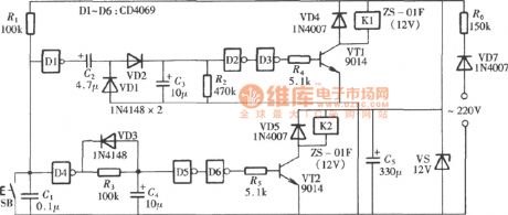
The Circuit of dual power switch that compose Of the CD4069
(View)
View full Circuit Diagram | Comments | Reading(776)
Three level circuit topology
Published:2011/4/21 2:16:00 Author:Nicole | Keyword: topology, three level
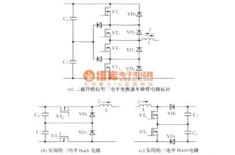
Traditional two level inverting bridge can be divided into Buck and Boost circuit easily, adopting a similar way, we can divede the diode-clamped three-level inverter as shown in figure (a) into three level Buck and Boost circuit with valuable, after necessary improvement. They are as shown in figure (b) and figure (c).
(View)
View full Circuit Diagram | Comments | Reading(649)
The configuration and pin circuit diagram of LM378
Published:2011/3/30 21:59:00 Author:Ecco | Keyword: configuration circuit, pin circuit

The configuration and pin circuit diagram of LM378 is as 7.46 shown. The main characteriatics: the supply is 10~35V, the output power is 4w, the input resistanceis 3kΩ, the gaining of voltage is 34dB, the bandwidth is 50KHz.
(View)
View full Circuit Diagram | Comments | Reading(445)
Infrared sensor music socket circuit diagram with SR5553
Published:2011/4/2 2:51:00 Author:Ecco | Keyword: Infrared sensor, music socket

View full Circuit Diagram | Comments | Reading(567)
Electronic dog triggered by footstep
Published:2011/4/1 1:45:00 Author:Ecco | Keyword: Electronic dog

View full Circuit Diagram | Comments | Reading(446)
Coded transmitting circuit diagram composed of TC9148
Published:2011/4/1 4:04:00 Author:Ecco | Keyword: Coded transmitting

Coded transmitting circuit diagram composed of TC9148 is as below:
TC91 series infrared remote controlling coded integrated circuit is a massive integrated circuit which adopts CMOS technology. And TC9148 is a coded transmitting circuit. TC9149 and TC9150 are topical empty receiving circuits. > (View)
View full Circuit Diagram | Comments | Reading(1899)
low power consumption single phase half-wave rectification capacitor filtering circuit diagram
Published:2011/4/20 21:16:00 Author:muriel | Keyword: low power consumption, single phase, half-wave rectification capacitor filtering

low power consumption single phase half-wave rectification capacitor filtering circuit diagram is as shown
(View)
View full Circuit Diagram | Comments | Reading(974)
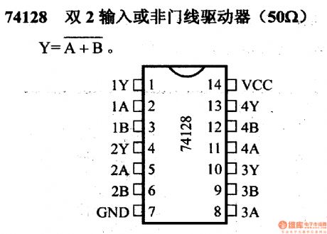
74 series digital circuit of 74128 double dual input or negater line driver(50Ω)
Published:2011/4/1 4:20:00 Author:Ecco | Keyword: digital circuit , double input , negater line driver
View full Circuit Diagram | Comments | Reading(693)
74 series digital circuit of 74S135 4 or gate/NOR gate
Published:2011/4/1 4:29:00 Author:Ecco | Keyword: digital circuit, or gate, NOR gate
View full Circuit Diagram | Comments | Reading(446)
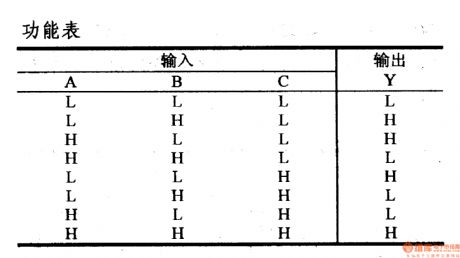
74 series digital circuit of 74HC131, 74LS131, 3 - 8 line decoder
Published:2011/4/2 3:51:00 Author:Ecco | Keyword: digital circuit , 3 - 8 line decoder
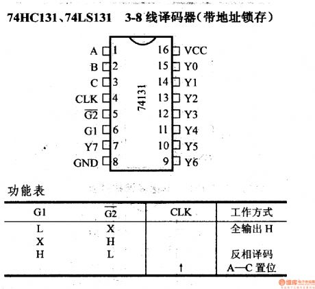
74 series digital circuit diagram of 74HC131, 74LS131, 3 - 8 line decoder(with address latching)is as below:
(View)
View full Circuit Diagram | Comments | Reading(3054)
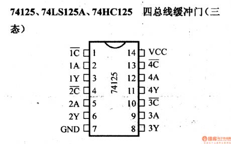
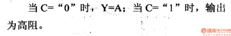
74 series digital circuit of 74125 74LS125A four buses buffer door(tristate)
Published:2011/4/2 3:52:00 Author:Ecco | Keyword: digital circuit, four buses buffer door
View full Circuit Diagram | Comments | Reading(1689)
74 series digital circuit of 74H102 input K- K negative edge trigger
Published:2011/4/2 4:04:00 Author:Ecco | Keyword: digital circuit, input K- K negative edge, trigger
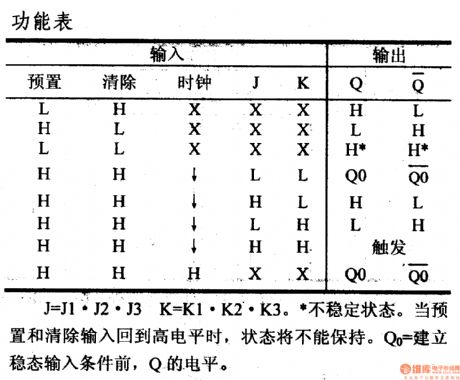
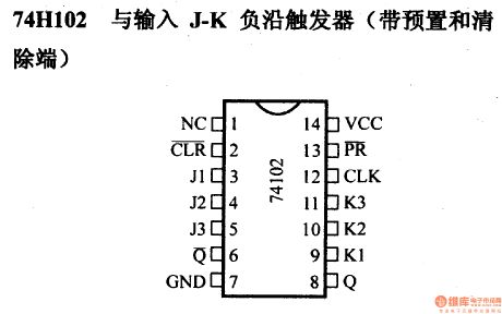
74H102 input K- K negative edge trigger( with preset and removr terminal)
Unsteady state. When the preset and remove terminal return in high level, the state could not be kept. And the level of Qo is equal to Q before eatablishing steadystate input. (View)
View full Circuit Diagram | Comments | Reading(531)
74 series digital circuit of 7492 74LS92 twelve frequency counter
Published:2011/4/2 4:04:00 Author:Ecco | Keyword: digital circuit, twelve frequency counter
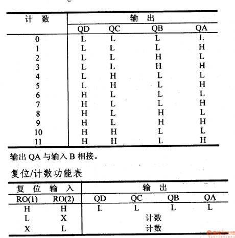
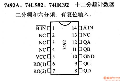
View full Circuit Diagram | Comments | Reading(3080)
74 series digital circuit of 74LS77 74HC77 4-bit bistable latch
Published:2011/4/5 22:54:00 Author:Ecco | Keyword: digital circuit , 4-bit, bistable , latch
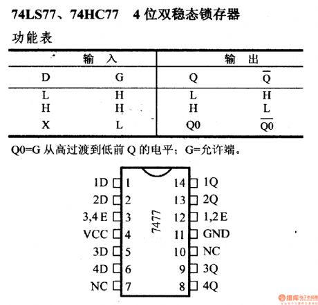
74LS77, 74HC77 4-bit bistable latch
The Q's level from Qo to G, which is from high level to low level: G=allowable terminal. (View)
View full Circuit Diagram | Comments | Reading(808)
74 series digital circuit of 7482 2-bit binary full adder
Published:2011/4/5 22:52:00 Author:Ecco | Keyword: digital circuit , 2-bit binary, full adder
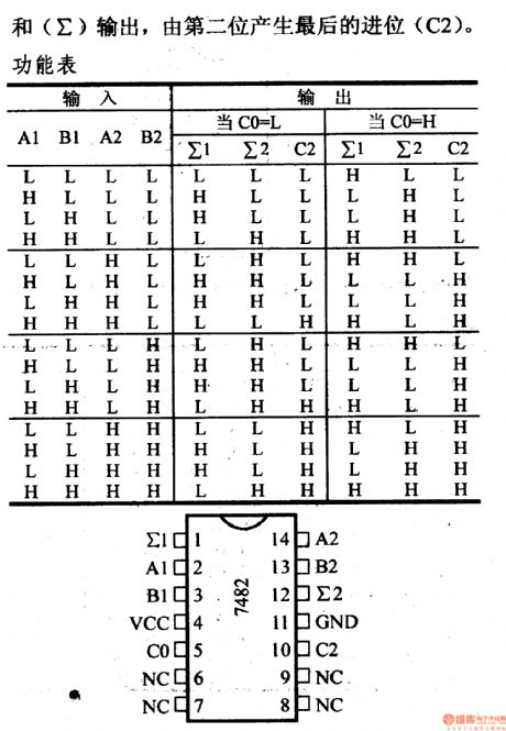

∑ output, and carry bit is produced by the second bit.
7482 2-bit binary full adder: To execute 2-bit binary addition. (View)
View full Circuit Diagram | Comments | Reading(3033)
| Pages:441/471 At 20441442443444445446447448449450451452453454455456457458459460Under 20 |
Circuit Categories
power supply circuit
Amplifier Circuit
Basic Circuit
LED and Light Circuit
Sensor Circuit
Signal Processing
Electrical Equipment Circuit
Control Circuit
Remote Control Circuit
A/D-D/A Converter Circuit
Audio Circuit
Measuring and Test Circuit
Communication Circuit
Computer-Related Circuit
555 Circuit
Automotive Circuit
Repairing Circuit