
Index 91
60_CPS_BANDSTOP_AMPLIFIER
Published:2009/7/10 5:05:00 Author:May

With fet as output buffer to give near-infinite load impedance, twin,T notch filter gives up to 50 db attenuafion at notch frequency.-FET's and RC Networks (Siliconix ad), Electronics, 39:4, p 71. (View)
View full Circuit Diagram | Comments | Reading(675)
HIGH_INPUT_IMPEDANCE_A_C_AMPLIFIER
Published:2009/7/10 5:05:00 Author:May

Gives input impedance of 30 meg without sacrificing bandwidth or noise performance.Voltage gain is 40 db, Technique involves bootstrapping fet Q1 and using fixed bias for its gate. Q2 is operoted grounded-base to reduce Miller capacitance of field effect at high frequencies.-Texus Instruments Inc., Transistor Circuit Design, McGraw-Hill,N.Y.,1963, p 520. (View)
View full Circuit Diagram | Comments | Reading(551)
445_KC_TUNNEL_DIODE_AMPLIFIER
Published:2009/7/10 5:02:00 Author:May

Has approximately 20 db gain.-I. A. Lesk, N. Ho-Ionyak, Jr, and u. s. Dovidsohn, The Tunnel Diode-Circuits and Applicalions, Electronics,32:48,p 60-64. (View)
View full Circuit Diagram | Comments | Reading(607)
65_CPS_AMPLIFIER
Published:2009/7/10 5:01:00 Author:May

Consists of three triode stages (V2A, V2B, and V3A). Peaks at about 6.5 cps, with 18 db attenuation at each octave. Double-T reiection filter between V2A and V2B ottenuates any 60-cps pickup. Overall gain is 80 db. Phase inverter V3B provides 180° out-of-phase signal for full-wave phose-sensitive bridge rectifier that uses reference signal.Output is rectified error signal for infrared analyzer used to detect leaks in automobile air-suspension systems.-P. G.Balko, Infrared Finds Auto Suspension Leaks, Electtonics, 31:49, p 82-85. (View)
View full Circuit Diagram | Comments | Reading(528)
ISOLATION_AMPLIFIER_1
Published:2009/7/10 4:59:00 Author:May

Effective gain stability factor is approximately equal to reciprocal of product of omplification factors of two halves of tube. Gives high transmission accuracy, with high input impedance.-G. M. Davidson and R. F. Brady, Unity-Gain Ampliler Offers High Stcability, Electronics, 33:9, p 66-67. (View)
View full Circuit Diagram | Comments | Reading(640)
ISOLATION_AMPLIFIER
Published:2009/7/10 4:58:00 Author:May

Gain stability and input impedance are much better than conventional cathode follower. Feedback capacitor goes between triode grids, but may also go between grid of V1B and cathode of V1A.-G. M. Davidson and R. F. Brady, Unity-Gain Amplifier Offers High Stability, Electronics, 33:9, p 66-67. (View)
View full Circuit Diagram | Comments | Reading(839)
SOLAR_CELL_AMPLIFIER
Published:2009/7/10 4:57:00 Author:May

Used with mulliaperture solar cells to genorate 10 strobe pulses.Eight circuits with cells one needed to generate 80 strobe pulses for reading conventional punched card.-C. R. Hearn,Multi-Aperture Solar Cell Amplifiter,EEE,14:4,p 43-44. (View)
View full Circuit Diagram | Comments | Reading(759)
CASCADED_741_OPAMPS
Published:2009/7/10 4:51:00 Author:May

Two opamps in series provide 80 dB of audio gain with bandwidth of about 300 to 6000 Hz. Gain of each opamp is set at 100. With three stages, bandwidth would be 5100 Hz. Output will drive loudspeaker at comfortable room level, if fed through 1-μF nonpolarized capacitor to output transformer having 500-ohm primaryand 8-ohm secondary.-C.Hall, Circuit Design with the 741 Op Amp, Ham Radio, April 1976, p 26-29. (View)
View full Circuit Diagram | Comments | Reading(887)
Sample_and_hold_circuit_used_to_automatically_zero_a_high_gain_amplifier
Published:2009/7/19 20:13:00 Author:Jessie
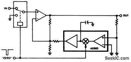
Sample-and-hold circuit used to automatically zero a high-gain amplifier (courtesy Analog Devices, Inc.). (View)
View full Circuit Diagram | Comments | Reading(552)
Notch_filter_using_an_ECG947_dual_operational_amplifier_as_a_gyrator
Published:2009/7/19 20:10:00 Author:Jessie
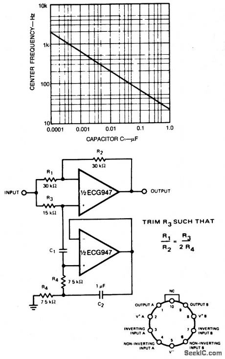
Notch filter using an ECG947 dual operational amplifier as a gyrator. The ECG947 is short-circuit protected and requires no external components for frequency compensation (courtesy GTE Sylvania Incorporated). (View)
View full Circuit Diagram | Comments | Reading(570)
A_F_AMPLIFIER_WITH_SQUELCH_2
Published:2009/7/17 22:40:00 Author:Jessie
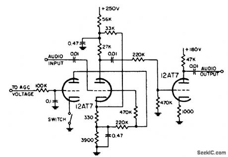
Used to make first audio stage inoperative during no-signal condition in communication receiver.-NBS, Handbook Preferred Circuits Navy Aeronautical Electronic Equipment, Vol. 1, Electron Tube Circuits, 1963, p N12-2. (View)
View full Circuit Diagram | Comments | Reading(627)
A_F_AMPLIFIER_WITH_SQUELCH_1
Published:2009/7/17 22:39:00 Author:Jessie

Input is obained from noise rectifier and amplifier of communication receiver. Squelch is used to make first audio stage inoperative during no-signal condition.-NBS, Handbook Preferred Circuits Navy Aeronautical Electronic Equipment, Vol, 1, Electron Tube Circuits, 1963, p N12-2. (View)
View full Circuit Diagram | Comments | Reading(653)
A_F_AMPLIFIER_WITH_SQUELCH
Published:2009/7/17 22:20:00 Author:Jessie

Used to make first audio stage inoperative during no-signal condition in communication receiver.-NBS, Handbook Preferred Circuits Navy Aeronautical Electronic Equipment, Vol. 1, Electron Tube Circuits, 1963, p N12-2. (View)
View full Circuit Diagram | Comments | Reading(659)
Voltage_follower_using_an_ECG915_operational_amplifier
Published:2009/7/19 21:39:00 Author:Jessie

Voltage follower using an ECG915 operational amplifier. Output is taken on pin 6 (courtesy GTE Sylvania Incorporated). (View)
View full Circuit Diagram | Comments | Reading(482)
Inverting_unity_gain_high_slew_rate_circuit_using_an_ECG915_operational_amplifier_
Published:2009/7/19 21:38:00 Author:Jessie

Inverting unity-gain high-slew-rate circuit using an ECG915 operational amplifier (courtesy GTE Sylvania Incorporated). (View)
View full Circuit Diagram | Comments | Reading(526)
Noninverting_op_amp_using_an_AD510_8_pin_TO99_
Published:2009/7/19 21:38:00 Author:Jessie

Noninverting op amp using an AD510 8-pin TO99 (courtesy Analog Devices, Inc.). (View)
View full Circuit Diagram | Comments | Reading(493)
Inverting_amplifier_using_half_of_an_ECG947_dual_operational_amplifier
Published:2009/7/19 21:37:00 Author:Jessie

Inverting amplifier using half of an ECG947 dual operational amplifier. The ECG947 is short-circuit protected and requires no external components for frequency compensation (courtesy GTE Sylvania Incorporated). (View)
View full Circuit Diagram | Comments | Reading(501)
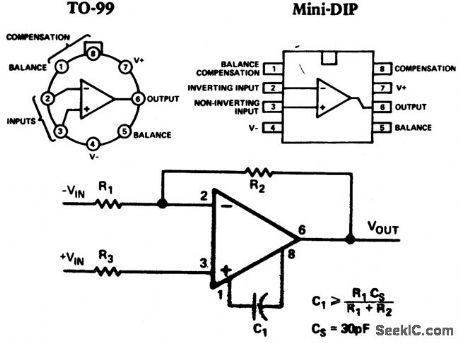
Op_amp_in_closed_loop_frequency_compensated_configuration_
Published:2009/7/19 21:36:00 Author:Jessie

Op amp in closed-loop frequency-compensated configuration (courtesy Motorola Semiconductor Products Inc.). (View)
View full Circuit Diagram | Comments | Reading(567)
Compressor_expander_amplifiers_using_an_ECG947_dual_operational_amplifier
Published:2009/7/19 21:35:00 Author:Jessie

Compressor/expander amplifiers using an ECG947 dual operational amplifier. The ECG947 is short-circuit protected and requires no external components for frequency compensation (courtesy GTE Sylvania Incorporated). (View)
View full Circuit Diagram | Comments | Reading(1376)
Single_pole_frequency_compensation_circuit_using_an_AD101A_201A_301A_op_amp
Published:2009/7/19 21:34:00 Author:Jessie
Single pole frequency compensation circuit using an AD101A/201A/301A op amp. Typical supply voltage is ±15volts. Voltage gain is 88 dB (courtesy Analog Devices, Inc.). (View)
View full Circuit Diagram | Comments | Reading(455)
| Pages:91/250 At 2081828384858687888990919293949596979899100Under 20 |
Circuit Categories
power supply circuit
Amplifier Circuit
Basic Circuit
LED and Light Circuit
Sensor Circuit
Signal Processing
Electrical Equipment Circuit
Control Circuit
Remote Control Circuit
A/D-D/A Converter Circuit
Audio Circuit
Measuring and Test Circuit
Communication Circuit
Computer-Related Circuit
555 Circuit
Automotive Circuit
Repairing Circuit