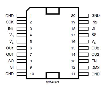
L9929, L9930, L9931 Selling Leads, Datasheet
MFG:ST Package Cooled:PowerSSO-24 D/C:07+

L9929, L9930, L9931 Datasheet download

Part Number: L9929
MFG: ST
Package Cooled: PowerSSO-24
D/C: 07+


MFG:ST Package Cooled:PowerSSO-24 D/C:07+

L9929, L9930, L9931 Datasheet download

MFG: ST
Package Cooled: PowerSSO-24
D/C: 07+
Want to post a buying lead? If you are not a member yet, please select the specific/related part number first and then fill the quantity and your contact details in the "Request for Quotation Form" on the left, and then click "Send RFQ".Your buying lead can then be posted, and the reliable suppliers will quote via our online message system or other channels soon.
TOP
PDF/DataSheet Download
Datasheet: L9929
File Size: 644909 KB
Manufacturer: STMICROELECTRONICS [STMicroelectronics]
Download : Click here to Download
PDF/DataSheet Download
Datasheet: L9930
File Size: 106040 KB
Manufacturer: STMICROELECTRONICS [STMicroelectronics]
Download : Click here to Download
PDF/DataSheet Download
Datasheet: L9903
File Size: 134408 KB
Manufacturer: STMICROELECTRONICS [STMicroelectronics]
Download : Click here to Download
The L9929 is an SPI controlled H-Bridge, designed for the control of DC and stepper motors in safety critical applications and under extreme environmental conditions.
The H-Bridge is protected against over temperature and short circuits and has an under voltage lockout for all the supply voltages "VS" (Main DC power supply). All malfunctions cause the output stages to go tristate.
The H-Bridge contains integrated free-wheel diodes. In case of free-wheeling condition, the low side transistor is switched on in parallel of its diode to reduce the current injected into the substrate. Switching in parallel is only allowed, if the voltage level of the according output-stage is below the ground-level. In this case it must be ensured, that the upper transistor is switched off.
The integrated circuit must not be destroyed by use at the limit values.
Each limit value can be used, as long as no other limit is violated.
Voltage reference point: All values are, if not otherwise stated, relative to ground.
Direction of current flow: Current flow into a pin is positive.
Rise-, fall- and delaytimes: If not otherwise stated, all rise times are between 10% and 90%, fall times between 90% and 10% and delay times at 50% of the relevant steps.
| Symbol | Parameter | Test Condition | Min. | Typ. | Max. | Unit |
| VS | Supply voltage | static destruction proof | -1 | 40 | V | |
| dynamic destruction proof t <0.5s (single pulse, Tj < 85°C) |
-2 | 40 | V | |||
| VLI | Logic inputs IN1, IN2, DI, EN, SS, SI, SCK,DMS |
-0.5 | 7 | V | ||
| VLO | Logic outputs SF, SO | -0.5 | 7 | V |

The L9930 is a dual full-bridge. The output stages are Power Mos switches.
| Symbol | Parameter | Value | Unit |
| E | Clamped Energy at the Switching off | 6 (max) | mJ |
| Vout DC | Continuous Output Voltage | 24 (max) | V |
| Vout tr | Transient Output Voltage | 32 (max) | V |
| Vbat DC | Continuous Battery Voltage | 8 to 24 | V |
| Vbat tr | Transient Battery Voltage | 45 (max) | V |
| Iout | Reverse Output Current | 2 (max) | A |
| fin | Input Frequency | 500 (max) | Hz |
| Vin | Input Voltage | 0.3 to +7 | V |
| Vdiag | Diagnostic Voltage | 0.3 to +7 | V |
| Ts | Storage Temperature | 55 to 150 | °C |
| Tj | Operating Junction Temperature | 40 to 150 | °C |
| VESD | VESD (Note MIL STD 883C) | 3000 | V |

