Want to post a buying lead? If you are not a member yet, please select the specific/related part number first and then fill the quantity and your contact details in the "Request for Quotation Form" on the left, and then click "Send RFQ".Your buying lead can then be posted, and the reliable suppliers will quote via our online message system or other channels soon.
Case temperature under bias:.........................-10 to +85 Storage temperature:....................................-65 to +125 Supply voltage with respect to VSS..................-0.2 V to 4.1 V Voltage On Any Pin (except VPP):-0.5 V to +VCC + 0.5 V(1,2,5) VPP voltage:........................................-0.5 V to +14.0 V (1,2,4) Output short-circuit current:.....................................100 mA(3)
*WARNING: Stressing the device beyond the ìAbsolute Maximum Ratingsi may cause permanent damage. These are stress ratings only. Operation beyond the ìOperating Conditionsi is not recommended and extended exposure beyond the ìOperating Conditionsi may affect device reliability.
82802AB Features
Intel platform compatability -Enables security-enhanced platform infrastructure; facilitates option to remove ISA. Firmware hub hardware interface mode - 5-Signal communication interface supporting byte-at-a-time reads and writes - Register-based read and write protection for each code/data storage block -Hardware write protect pins for the top boot block and the remaining code/data storage blocks -5 Additional GPIs for platform design flexibility - Contains a hardware Random Number Generator (RNG) for enhancing platform security -Integrated Command User Interface (CUI) for requesting access to locking, programming, and erasing options. The CUI also handles requestsfor data residing in status, ID, and block-lock registers. -Operates with 33-MHz PCI clock and 3.3 V I/O. Industry-standard packages (40L TSOP or 32L PLCC) Two configurable interfaces -Firmware hub interface for platform operation - Address/Address-Multiplexed (A/A Mux) interface for programming during manufacturing 4 or 8 Mbits of flash memory for platform code/data nonvolatile storage -Symmetrically blocked, 64-KB memory sections - Available in 8-Mbit (Intel® 82802AC) and 4-Mbit (Intel® 82802AB) densities - Automated byte program and block erase via an integrated Write State Machine (WSM) Address/Address-Multiplexed (A/A Mux) interface/mode -11-Pin multiplexed address and 8-pin data I/O interface -Supports fast on-board or out-of-system programming for manufacturing Case temprature operating range Power supply specifications -Vcc: 3.3 V ± 0.3 V - Vpp: 3.3 V and 12 V for fast programming, (80 hours maximum)
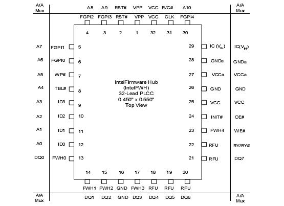
82802AB Connection Diagram
The pin descriptions table details the usage of each device pin. Most pins have dual functionality, with functions in both the Intel Firmware Hub and A/A Mux interfaces. The A/A Mux functionality for pins is shown bold italic in the description box for that pin. All pins are designed to be compliant with VCC + 0.3 V max. unless otherwise noted.
82802AC Maximum Ratings
Case temperature under bias:.........................-10 to +85 Storage temperature:....................................-65 to +125 Supply voltage with respect to VSS..................-0.2 V to 4.1 V Voltage On Any Pin (except VPP):-0.5 V to +VCC + 0.5 V(1,2,5) VPP voltage:........................................-0.5 V to +14.0 V (1,2,4) Output short-circuit current:.....................................100 mA(3)
*WARNING: Stressing the device beyond the ìAbsolute Maximum Ratingsi may cause permanent damage. These are stress ratings only. Operation beyond the ìOperating Conditionsi is not recommended and extended exposure beyond the ìOperating Conditionsi may affect device reliability.
82802AC Features
Intel platform compatability -Enables security-enhanced platform infrastructure; facilitates option to remove ISA. Firmware hub hardware interface mode - 5-Signal communication interface supporting byte-at-a-time reads and writes - Register-based read and write protection for each code/data storage block -Hardware write protect pins for the top boot block and the remaining code/data storage blocks -5 Additional GPIs for platform design flexibility - Contains a hardware Random Number Generator (RNG) for enhancing platform security -Integrated Command User Interface (CUI) for requesting access to locking, programming, and erasing options. The CUI also handles requestsfor data residing in status, ID, and block-lock registers. -Operates with 33-MHz PCI clock and 3.3 V I/O. Industry-standard packages (40L TSOP or 32L PLCC) Two configurable interfaces -Firmware hub interface for platform operation - Address/Address-Multiplexed (A/A Mux) interface for programming during manufacturing 4 or 8 Mbits of flash memory for platform code/data nonvolatile storage -Symmetrically blocked, 64-KB memory sections - Available in 8-Mbit (Intel® 82802AC) and 4-Mbit (Intel® 82802AB) densities - Automated byte program and block erase via an integrated Write State Machine (WSM) Address/Address-Multiplexed (A/A Mux) interface/mode -11-Pin multiplexed address and 8-pin data I/O interface -Supports fast on-board or out-of-system programming for manufacturing Case temprature operating range Power supply specifications -Vcc: 3.3 V ± 0.3 V - Vpp: 3.3 V and 12 V for fast programming, (80 hours maximum)
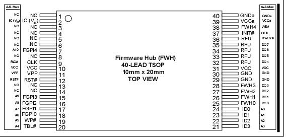
82802AC Connection Diagram
The pin descriptions table details the usage of each device pin. Most pins have dual functionality, with functions in both the Intel Firmware Hub and A/A Mux interfaces. The A/A Mux functionality for pins is shown bold italic in the description box for that pin. All pins are designed to be compliant with VCC + 0.3 V max. unless otherwise noted.