About SeekIC | Services | Payment | Advertisements service | Contact Us | Links
© 2008-2012 SeekIC.com Corp.All Rights Reserved.

Published:2009/7/22 1:06:00 Author:Jessie
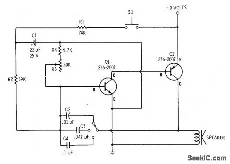
Tone is made adjustable by using multiposition switch to change capacitors in oscillator circuit. Speed (rate of change in frequency) of siren is adjusted with R3. 4700-ohm resistor in series with R3 keeps siren op-erational when R3 is rotated to minimum-resistance position. Siren is operated by pressing switch to produce rising wail, then releasing switch until wail drops down to cutoff.-F. M. Mims, Transistor Projects, Vol.1, Radio Shack, Fort Worth, TX, 1977, 2nd Ed., p 58-63. (View)
View full Circuit Diagram | Comments | Reading(916)
Published:2009/7/6 21:42:00 Author:May

Pulse output is obtained from Exar XR-2006C functiongenerator l0 when pin 9 is shorted to squarewave output at pin 11. Pulse duty cycle, along with rise and fall times of ramp from pin 2, is determined by values of R1 and R2. Both can be adiusted from 1 to 99% by proper selection of resistor values as given in formulas alongside diagram.-E. NoLL VHF/UHF Single-Frequency Conversion, Ham Radio, April 1975, p 62-67. (View)
View full Circuit Diagram | Comments | Reading(738)
Published:2009/7/22 1:06:00 Author:Jessie

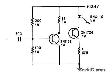
Linear range of 80% modulation for bandwidth of 30 cps to 250 kc, with only 3% distortion at 1 kc, permits good voice transmission over light beams generated by SNX110 Iight-emining diode.-E. L. Bonin, Drivers for Optical Diodes, Electronics, 37:22, p 77-82. (View)
View full Circuit Diagram | Comments | Reading(1086)
Published:2009/7/6 21:40:00 Author:May
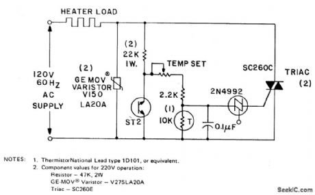
The circuit can control up to 6 kW of heating, with moderate gain,using a 25-amp triac(SC260D). Feedback is provided by the negative temperature co-efficient(NTC)thermistor,which is mounted adjacent to the environment being temperature controlled.The temperature set potentiometer is initially adjusted to the desired heating level.As the thermistor becomes heated by the load ,its resistance drops,phasing back the conduction angle of the triac,so the load voltage is reduced.The ST2 diac is used as a back-to-back ziner diode.Its negativeresistance region in its E-I characteristic Provides a degree of line vdtage stabilization. As the input line voltage increases,the diac triggers earlier in the cycle and, hence, the average charging voltage to the 0.1 μF capacitor,decreases. (View)
View full Circuit Diagram | Comments | Reading(4515)
Published:2009/7/6 21:40:00 Author:May
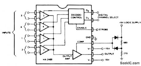
When operated as an open loop without compensation, the HA-2400 becomes a comparator with four selectable input channels. The clamping network at the compensation pin limits the output voltage to allow DTL or TTL digital circuits to be driven with a fanout of up to ten loads.
The circuit can be used to compare several signals against each other or against fixed references; or a single signal can be compared against several references. A window comparator, which assures that a signal is within a voltage range, can be formed by monitoring the output polarity, while rapidly switching between two channels with different reference inputs and the same signal input. (View)
View full Circuit Diagram | Comments | Reading(629)
Published:2009/7/22 1:05:00 Author:Jessie
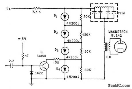
Uses four Shockley diodes in series, triggered by avalanche triode transistor, to give action similar to that of conventional line-type pulser using hydro gen thyratron, but requires no heater power or warmup.-L. Diven, Solid-State Modulator Feeds Subminiature Transponder, Electronics, 33:27, p 48-51. (View)
View full Circuit Diagram | Comments | Reading(1412)
Published:2009/7/6 21:39:00 Author:May
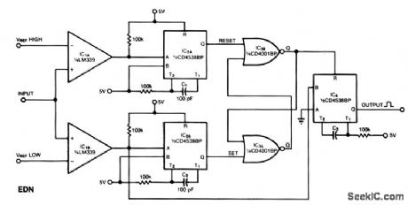
This window comparator generates an output pulse for each event that occurs within a specified window. That is, each output pulse signifies an input voltage pulse or level change that exceeds VREFLOW, but not VREFHIGH. The monostable multi ibrators, IC2A and IC2B, produce a 10-μS pulse at their Q output in response to a rising edge at their A input. Comparator IC1B produces a rising edge when the input exceeds VREFLOW, and comparator IC2A produces a rising edge when the input exceeds VREFHIGH. The NOR gates, IC3A and IC3B, form a bistable latch whose Q output, when low, disables IC4. IC4, unless disabled, produces output pulses in response to falling edges at the IC1B comparator output. You set the width of these pulses by selecting the value of C3. The circuit can handle an input waveform containing 0 to 2 V amplitudes and 10-Hz to 10-kHz frequency components. (View)
View full Circuit Diagram | Comments | Reading(0)
Published:2009/7/22 1:02:00 Author:Jessie
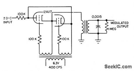
Dual-triode performs chopper function. With 6.3 v rms carrier, output is linear to 2 v rms for d-c inputs up to 25 v. Null level is 100 my, but can be reduced by filtering. Long-time drift stability is excellent. Output signal is nor molly square-wave, but tuned circuit shown converts this to sinusoidal signal.-L. S.Klivans, Modulators for Automatic Control Systems, Electronics, 31:1, p 82-84. (View)
View full Circuit Diagram | Comments | Reading(722)
Published:2009/7/22 0:49:00 Author:Jessie

This figure shows the circuit and corresponding waveforms for a unijunction transistor oscillator (Fig. 5-41). When Vs is pure dc, the oscillator is free-running and RT/CT determine the frequency of oscillation. Figure 9-1B shows the basic relaxation oscillator, whore the output pulses are synchronized to the line-voltage zero-crossing points. Typical values (for a UJT with a base-to-base voltage of 4 to 9 V) are:RB1=40 to 100 Ω, RB2 1 kΩ, CT=0.1μF, RT= 100 kΩ. (View)
View full Circuit Diagram | Comments | Reading(1935)
Published:2009/7/6 21:39:00 Author:May
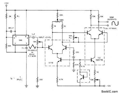
Nonlinear emitter-base junction characteristic of 511B transistorarray is used for shaping triangle output of 566 function generator to give sine output having less than 2% distortion. Amplitude of triangle is critical and must be carefully adjusted for minimum distortion of sine wave by varying values of R1, R2, and input level pot while monitoring output with Hewlett-Packard 333A distortion analyzer.- Signetics Analog Data Manual, Signetics, Sunnyvale, CA, 1977, p 851-853. (View)
View full Circuit Diagram | Comments | Reading(1066)
Published:2009/7/22 0:37:00 Author:Jessie
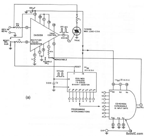
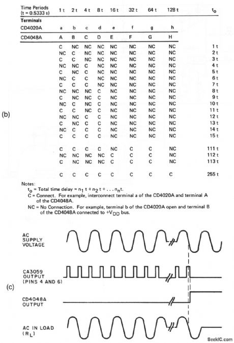
This circuit provides precise current through a load, as determined by a pulsed triac. The circuit is programmable over the range from 0.5333 s to 2 min and 16s, in 0.5333-s intervals. Figure 8-41B shows the connections for the various time intervals, and Fig. 8-41C shows the timing diagram. (View)
View full Circuit Diagram | Comments | Reading(661)
Published:2009/7/6 21:38:00 Author:May
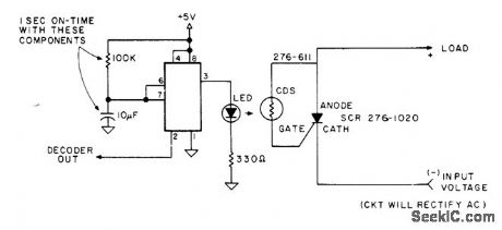
Decoder output of microprocessor feeds 555 timer driving LED that is mounted in light shield with cadmium sulfide photocell. Combination serves as optocoupler for triggering gate of SCR to energize load for short time interval determined by value of resistor and capacitor used. Serves to control small DC motor such as is used to raise or lower transmitter power in small increments.-R. Wright, Utilize ASCII Control Codes!, Kilobaud, Oct. 1977, p 80-83. (View)
View full Circuit Diagram | Comments | Reading(1206)
Published:2009/7/22 0:33:00 Author:Jessie
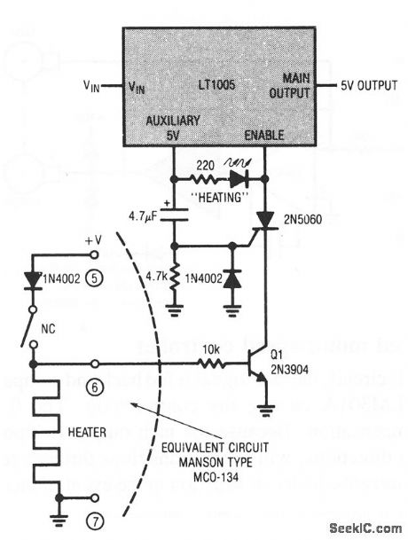
This circuit combines an LT1005 multifunction regulator and a typical commercial crystal oven to prevent equipment use until oven temperature has stabilized (as is often required in precision test equipment). When power is applied, pin 6 of the crystal oven is high, which biases Q1 on. Simultaneously, the SCR gate is triggered by the current flowing through the 4.7-kΩ resistor (the 4.7-μF capacitor charge current). This turns the SCR on and allows the load (the LT1005 enable pin) to receive power. The 4.7-kΩ resistor eliminates false SCR triggering, and the diode suppresses reverse gate current when LT1005 input power is removed. (View)
View full Circuit Diagram | Comments | Reading(734)
Published:2009/7/6 21:38:00 Author:May


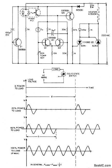
The zero voltage switching technique is widely used to modulate heating and similartypes of ac loads where the time constant associated with the load(tens of seconds tominutes) is sufficiently long to allow smooth proportional modulation by time ratio control,usmg one complete cycle of the ac input voltage as the mlnlmum switching movementoDespite its attractions,the traditional triac-based ZVS is virtually unusable for the controlof very low power loads,especially from 220 volt ac inputs due to the triac's reluctanceto latch-on into the near-zero instantaneous currents that flow through it and the loadnear the ac voltage zero crossover point so The circuit side-steps the latching problem by employing a par of very sensitive low current reverse blocking thyristors(C106)connected in antiparallel;these are triggered by a simple thermistor modulated differential amplifier(Q1,Q2),with zero voltage logic furnished by an H11AA1 ac input optocoupleroWith the NTC thermistor TH calling for heat,transistor Q1 is cut off and Q2 is on,which would normally provide contmuous base drive to Q3,with consequent triggeing of either SCR,or of SCR 2 vla SCR1,depending on phasing of the ac input.Note that when the ac input voltage is positive with respect to SCR 2,SCR 1 isreverse biased and,in the presence of gate current from Q3,behaves as a remotebase transistor, whose output provides vla blocking diode CR1,positive gate triggercurrent for SCR 2.When the ac input polarity is reversed(SCR 1's anode positive),SCR 1 behaves as a direct fired conventional thyristoro Trigger current to SCR 1,however,is not continuous,even when TH is calling for heat and Q2 is delivering basecurrent to Q3.In this situation,Q3 is inhibited from conduction by the clamping actionof POI,an H11AA photocoupler,except during those brief instants when the ac input voltage is near zero and the coupler input diodes are deprived of current.Triggering of either SCR can occur Only at ac voltage crosslng points,and RFI-less operation resultsoThe proportional control feature is injected via the positive feedback action of capacitor CM,which converts the differential amplifier Q1,Q2 into a simple multivibrator,whose duty cycle vanes from one to 99 percent according to the resistance of TH.Zener diode 21 is operational,being preferred when maxlmum immunity from ac voltage induced temperature drift is desired. (View)
View full Circuit Diagram | Comments | Reading(1849)
Published:2009/7/22 0:26:00 Author:Jessie
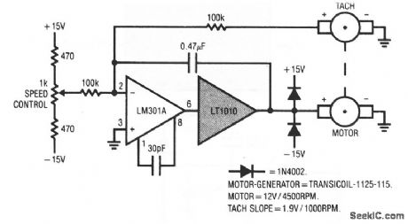
With this circuit, the tach signal is fed back and compared to a reference current, with the LM301A closing the control loop. The 0.47-μF capacitor provides stable compensation. Because the tach output is bipolar, the speed is controllable in both directions, with clean transitions through zero. The LT1010 thermal protection prevents device destruction in the event of mechanical overload or malfunction. (View)
View full Circuit Diagram | Comments | Reading(611)
Published:2009/7/6 21:35:00 Author:May
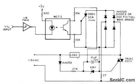
Output of. microprocessor drives LED of photocoupler through one section of 7414 hex Schmitt-trigger-input inverter. Output of phototransistor controls SCR connected across full-wave diode bridge. Current flow through bridge and SCR turns on triac, allowing alternating current to flow through load, Choose triac rated for handling required load current.-M. Boyd, Interfacing Tips, Kilo-baud, Feb. 1978, p 72-74. (View)
View full Circuit Diagram | Comments | Reading(1378)
Published:2009/7/6 21:35:00 Author:May

When the upper or lower limit is exceeded, the LED lights up. Positive feedback to one of the nulling terminals creates 5 to 20 μV of hysteresis on both amplifiers. This feedback changes to offset voltage of the LT1002 by less than 5μV . Therefore, the basic accuracy of the comparator is limited only by the low offset voltage of the LT1002.
(View)
View full Circuit Diagram | Comments | Reading(677)
Published:2009/7/6 21:34:00 Author:May

The circuit provides complete, linearized signal conditioning for a platinum RTD.This LTC1043 based circuit is considerably simpler than instrumentation or multi-amplifier based designs, and will operate form a single 5 V supply. A1 serves as a voltage-controlled ground referred current source by differentially sensing the voltage across the 998 phm feedback resistor. The LTC1043 section which does this presents a single-ended signal to A1's negative input, closing a loop. The 2 k 0.1 μF combination sets amplifier roll-off well below the LTC1043's switching frequency and the configuration is stable. Because A1's loop forces a fixed voltage across the 887 ohm resistor, the current through Rp is constant. A1's operating point is primarily fixed by the 2.5 V LT1009 voltage reference. (View)
View full Circuit Diagram | Comments | Reading(621)
Published:2009/7/22 0:09:00 Author:Jessie
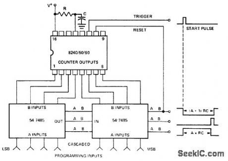
Electronically programmed timer using an Intersil 8240/50/60 16-pin DIP. This circuit uses a standard 54/74 series TTL 4-bit magnitude comparator to compare the digitally programmed input with the 8240/50/60 counter outputs. The greater, less-than and equal waveforms provide several outputs to choose from. An external start pulse triggers the timer and the A<B output is used as a reset (courtesy Intersil, Inc.). (View)
View full Circuit Diagram | Comments | Reading(1659)
Published:2009/7/22 0:05:00 Author:Jessie
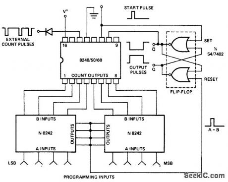
Electronically programmed counter using the Intersil 8240/50/60 16-pin DIP. Two quad exclusive-NOR circuits with open-collector outputs are wired together to form an inexpensive digital comparator. A start pulse triggers the 8240/50/60 counter and sets the output flip-flop high. The digital comparator output goes high momentarily when A is equal to B. This resets the flip-flop, which in turn resets the counter. For extended temperature range or higher speed operation individual pull-up resistor may be required on the counter outputs (courtesy Intersil, Inc.). (View)
View full Circuit Diagram | Comments | Reading(1364)
| Pages:1015/2234 At 2010011002100310041005100610071008100910101011101210131014101510161017101810191020Under 20 |
Response in 12 hours
© 2008-2012 SeekIC.com Corp.All Rights Reserved.