
Circuit Diagram
Index 1009
PRECISION_ONE_SHOT
Published:2009/7/7 0:51:00 Author:May


If you need a wide-range, resistor-programmable monostable multivibrator, you can program the circuit for pulse widths from 1 μs to 10s-107:1 range. A high-to-low transition at the input causes IC1's output to switch low, thereby turning off Q1 and Q2. With the latter transistor turned off, IC3's output increases and the output of IC2 begins to ramp toward the negative supply level at a rate determined by the 0.01-μF capacitor and the programming resistor. When IC2's output voltage reaches -5 V, IC3's output switches low. If you anticipate input pulses shorter than the desired output pulses, Q3 is necessary. This transistor keeps IC1s input low while an output pulse is present, thereby preventing inadvertent resetting of the one shot. (View)
View full Circuit Diagram | Comments | Reading(781)
20_METER__DIRECT_CONVERSION
Published:2009/7/21 22:37:00 Author:Jessie

Well-designed circuit provides pleasing polarity and depth of sound, with SSB signals seeming to stand out against nearly noiseless background. Covers entire 20-meter band. Use of balanced-product detector improves stability to reject strong broadcast-band AM signals. BFO energy from Q4 is injected through center tap of broad-band toroidal transformer L4-L5. Except for preselector, selectivity is obtained only through shaping of audio channel. Bandwidth is more appropriate for CW if C7 is increased to 0.02 or 0.047μF. T1 is 10K to 2K CT Stancor TAPC-35.L2 is 40 turns No. 30 enamel on T-37.6 core, with 2 turns No. 28 on it for L1 and 4 turns for L3. L5 is 16turns No. 28 on FT-37-63 core, with center tap, with 4turns No.28 on it for L4, L6is 19turns No. 28 on 7-37-6 core, tapped 7 turns above ground.-J. Rusgrove, A 20-Meter High-Performance Direct-Conversion Receiver, OST, April 1978, p 11-13. (View)
View full Circuit Diagram | Comments | Reading(3322)
TAPE_LOOP_SPEED_CONTROL
Published:2009/7/7 0:01:00 Author:May
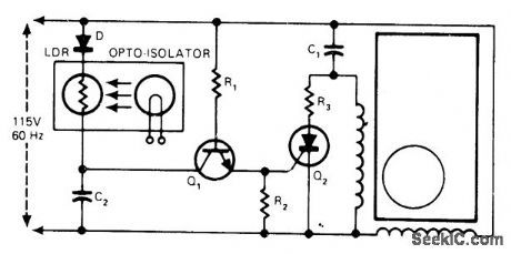
Shunt rectifier-capacitor circuit was developed for speed control of permanent split-capacitor fractional-horsepower induction motor used in some motion-picture projectors. Light-dependent resistor UDR makes Q2 conduct when light from lamp is not blocked by tape loop. Split capacitor C1 for motor provides both run and speed-control functions without switching. Values are: C2 0.01μF; D 1N4004; Q1 2N4987; Q2 C106B; R1 330K; R2 100; R3 10.-T. A. Gross, Control the Speed of Small Induction Motors, EDN Magazine, Aug. 20, 1977, p 141-142. (View)
View full Circuit Diagram | Comments | Reading(1613)
2_hp_THYRISTOR_CONTROL
Published:2009/7/6 23:57:00 Author:May
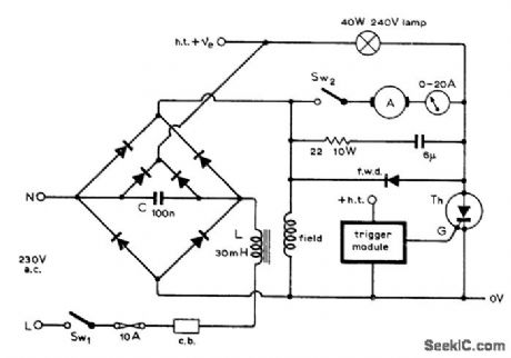
Provides smooth variation in speed of shunt-wound DC motor from standstill to 90% of rated speed. Use thyristor rated 30 A at 600 V. Outer diodes of bridge are 35-A 600-PIV silicon power diodes, as also is thyristor diode, and inner diodes are 5-A 600-V silicon power diodes. Article gives complete circuit of trigger pulse generator used to control speed by varying duty cycle of thyristor. Larger motors can be controlled similarly by uprating thyristor and diodes. Controller will also handle other types of loads, including lamps and heaters.-F. Butler, Thyristor Control of Shunt-Wound D.C. Motors, Wireless World, Sept. 1974, p 325-328. (View)
View full Circuit Diagram | Comments | Reading(1586)
Fluorescent_starter
Published:2009/7/21 22:36:00 Author:Jessie

This circuit shows a solid-state fluorescent-lamp starter that uses a SIDAC. In this circuit, the ballast is identical to that used with a conventional glow-tube starter. (View)
View full Circuit Diagram | Comments | Reading(2806)
MOSFET_PRODUCT_DETECTOR
Published:2009/7/21 22:34:00 Author:Jessie
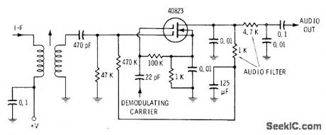
SSB IF signal is applied to one gate of MOSFET and demodulating carrier to other gate. Linear demodulation is obtained without distortion components. RC filter connected into drain circuit removes IF and carrier components, leaving de-modulated audio as output.-E. M. Noll, FET Principles, Experiments, and Projects, Howard W. Sams, Indianapolis, IN, 2nd Ed., 1975, p 154. (View)
View full Circuit Diagram | Comments | Reading(1008)
Xeon_flasher
Published:2009/7/21 22:34:00 Author:Jessie

This circuit shows an xeon tube triggered by a SIDAC that is connected as a basic relaxation oscillator, where the frequency is determined primarily by the RC time constant (a SIDAC relaxation oscillator is shown in Fig. 5-40). Once the capacitor voltage reaches the SIDAC breakover voltage (as determined by the setting of the series potentiometer), the SIDAC fires, and dumps the charged capacitor. By placing the load (transformer-coupled xeon tube) in the discharge path, the flashing frequency can be controlled. (View)
View full Circuit Diagram | Comments | Reading(2158)
250_mW_FOR_40_METER_CW
Published:2009/7/6 23:53:00 Author:May

Two-transistor circuit is easily assembled on circular printed-circuit board small enough to fit into tunafish can, for low-power (QRP) operation. Simple Pierce crystal oscillator 01 feeds class C ampli-fier 02. La is made by unwinding 10-μH Radio Shack choke 273-101 and filling form with No. 28 or 30 enamel to give 24 μH. Similar choke is unwound so only 11 turns remain (1.36 μH), with turns spaced one wire thickness apart for L2. Adjustspacing of turnsfor maximum output during final tune-up with transmitter operating into 50-ohm load. Fortl, remove all but 50 turns from 100-μH Radi. Shack choke 273-102 andwind 25 turns No,22 or 24 Henamel over these,Supply can be nlne Penlite, C, or D cells in seriesor 12-V or13-V regulated DC supply al and a2 are 2N2222A or equivalent Y1 is 7-MHz fundamental crysta:-D,DeMaw'Build a Tuna-Tin 2, QST, May 1976, p 14-16. (View)
View full Circuit Diagram | Comments | Reading(1174)
TRANSISTOR_CURVE_TRACER_1
Published:2009/7/21 22:33:00 Author:Jessie

Staircase wave-form generator supplies lest transistor with six values of base current during etch cycle, to develop family of curves for cro. Range switches give wide choice of test voltages and currents. Four-layer and tunnel diodes can also be checked.-C. J. Candy, Simplified Curve Tracer for Transistors and Diodes, Electronics, 33:34, p 68-70. (View)
View full Circuit Diagram | Comments | Reading(4163)
PWM_SPEED_CONTROL
Published:2009/7/6 23:53:00 Author:May
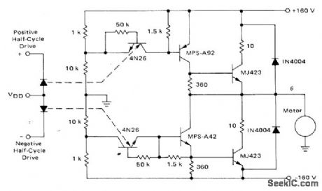
Power stage using Motorola 4N26 optoisolators and push-pull transistors drives fractional -horsepower single-phase AC motor over speed range of 5% to 100% of base speed. Input drives are provided by pulse-width modulation inverter using stored program in ROM to generate sine-weighted pulse trains to provide variable-frequency drive.-T. Mazur, ”ROM-Digital Approach to PWM-Type Speed Control of AC Motors,”Motorola, Phoenix, AZ, 1974, AN-733, p12. (View)
View full Circuit Diagram | Comments | Reading(2879)
SWITCHING_MODE_CONTROLLER
Published:2009/7/6 23:49:00 Author:May
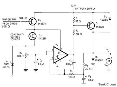
Developed for driving 0.0l-hp motor M at variable speeds with minimum battery drain. Circuit uses pulses with low duty cycle to set up continuous current in motor approximating almost 200 mA when average battery drain is 100 mA for output volt-age of 3.5 V. Voltage comparator A, serves as oscillator and as duty-cycle element of controller. C1 and R1 provide positive feedback giving oscillation at about 20 kHz, with duty-cycle range of 10% to 70% controlled by feedback loop Q1-R1-C3-R3. D2 is used in place of costly large capacitor for filtering.-J. C. Sinnett, Switching-Mode Controller Boosts DC Motor Efficiency, Electronics, May 25, 1978, p 132. (View)
View full Circuit Diagram | Comments | Reading(674)
10_MHz_universal_counter_using_the_Intersil_ICM7216B_28_pin_DIP
Published:2009/7/21 23:14:00 Author:Jessie

10 MHz universal counter using the Intersil ICM7216B 28-pin DIP. This circuit can use input frequencies up to 10MHz at input A and up to 2 MHz at input B (courtesy Intersil, Inc.). (View)
View full Circuit Diagram | Comments | Reading(1429)
10_MHz_PRODUCT_DETECTOR
Published:2009/7/21 23:13:00 Author:Jessie
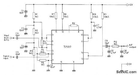
IF signal of SSB receiver is mixed with signal from beat-frequency oscillator in Mullard TCA240 dual balanced modulator-demodulator to give desired audio output signal, Simple low-pass filter R12-C9-C10 removes unwanted output signal.- Applications of the TCA240, Mullard, London, 1975, Technical Note 18, TP1489. (View)
View full Circuit Diagram | Comments | Reading(2520)
SINGLE_SUPPLY_PRODUCT_DETECTOR
Published:2009/7/21 23:11:00 Author:Jessie
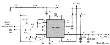
Motorola MC1596G balanced modulator requires no carrier null adjustment because all frequencies except desired demodulated audio are in RF spectrum and easily filtered out. Circuit performs well with carrier input levels of 100-500mVRMS. Provides good product detector performance from very low frequencies up to 100MHz.-R Hejhall, MC1596 Balanced Modulator,Motorola.Phoenix.AZ,1975.AN-531,p7. (View)
View full Circuit Diagram | Comments | Reading(774)
UNTUNED_DOUBLE_BALANCED_MIXER
Published:2009/7/21 23:10:00 Author:Jessie
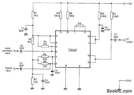
Wideband mixer for high-frequency SSB circuits operates from single 12-V supply. Gain is controlled by R9 and increases as value of R9 is decreased. Output at pins 13 and 14 is product of local oscillator and signal input frequencies and contains desired IF value for receiver. Oscillator signal level should be kept below 20 mV to avoid undesired harmonics produced by limiting. Circuit uses Mullard TCA240 dual balanced modulator-demodulator.- Applications of the TCA240, Mullard, London, 1975, Technical Note 18, TP1489. (View)
View full Circuit Diagram | Comments | Reading(1106)
SCR_control_circuit_with_dc_output_that_uses_an_SBS
Published:2009/7/21 23:10:00 Author:Jessie

This circuit is similar to that of Fig. 8-25, except that a provided to the load. With MCR3818-4 controlled rectifiers mounted heatsink, this circuit will control up to 3-kW power froma 120-V line. (View)
View full Circuit Diagram | Comments | Reading(942)
TWO_TONE_TESTER
Published:2009/7/21 23:09:00 Author:Jessie

Twin-T transistor oscillators generate two distinct sine-wave AF signals for use in adjusting SSB transmitters. Q1 is fixed at about 1000 Hz, and Q2 is adjustable between 1000 and 1300 Hz, giving frequency difference of 0-300 Hz for use with scopes having 60-Hz horizontal sweep rate that permits display of one to five cycles of RF envelope pat-tern. Switches permit use of either oscillator separately.-F. Brown, The Two-Tone Tester, QST, Nov, 1978, p 22-24. (View)
View full Circuit Diagram | Comments | Reading(1253)
Ultralong_delay_timer_using_two_8240_16_pin_DIPs
Published:2009/7/21 23:07:00 Author:Jessie

Ultralong delay timer using two 8240 16-pin DIPs. The time base of unit 2 is disabled. The output is normally high when the system is reset. Upon application of a trigger the output goes low and stays that way for a duration of (256)2 or 65,536 cycles of the time base oscillator. Total timing cycle of the circuit is programmed from To = 256RC to To = 65,536RC in 256 discrete steps by selecting any combination of the counter outputs of unit2 (courtesy Intersil, Inc.). (View)
View full Circuit Diagram | Comments | Reading(703)
Basic_SCR_control_circuit_that_uses_an_SBS
Published:2009/7/21 23:07:00 Author:Jessie

This figure shows the basic control circuit for SCRs that use SBS triggers, and is preferable to that of Fig. 8-24 (triac), where high power must be handled, or whore rapidly rising voltages are encountered (high dv/dt,). Although the circuits of both Figs. 8-24 and 8-25 were designed as incandescent-lamp dimmers, the circuits are well suited to control of universal and shaded-pole motors. Such motors have higher torque at low speeds when open-loop controlled by these circuits, rather than with rheostats or variable transformers (because of the higher voltage pulses applied). (View)
View full Circuit Diagram | Comments | Reading(970)
Digital_sample_and_hold_circuit
Published:2009/7/21 23:06:00 Author:Jessie

Digital sample-and-hold circuit. When a strobe input is applied the 8240/8250 is first reset, then triggered through the small RC network at pin 11, which delays the strobe signal. The strobe also sets the flip-flop, which in turn enables the counter via pin 14. The op amp goes to the high state and begins to countdown at a rate set by the counter time base. When the op amp output reaches the analog input to be sampled the comparator switches, resetting the flip-flop and stops the count. The op amp output will accurately hold the sampled value until the next strobe pulse is applied. If the time base here is used the maximum acquisition time would be 256 (8240, 100 for the 8250) times 0.01 ms, or 2.6 ms (courtesy Intersil, Inc.). (View)
View full Circuit Diagram | Comments | Reading(1651)
| Pages:1009/2234 At 2010011002100310041005100610071008100910101011101210131014101510161017101810191020Under 20 |
Circuit Categories
power supply circuit
Amplifier Circuit
Basic Circuit
LED and Light Circuit
Sensor Circuit
Signal Processing
Electrical Equipment Circuit
Control Circuit
Remote Control Circuit
A/D-D/A Converter Circuit
Audio Circuit
Measuring and Test Circuit
Communication Circuit
Computer-Related Circuit
555 Circuit
Automotive Circuit
Repairing Circuit