
Circuit Diagram
Index 1013
AMPLITUDE_MODULATOR
Published:2009/7/6 22:27:00 Author:May
Motorola type MC1596G balanced modulator functions as amplitude modulator when carrier null is unbalanced enough to insert proper amount of carrier into output signal. Provides excellent modulation from 0% to well over 100%.-R. Hejhall, MC1596 Balanced Modulator, Motorola, Phoenix, AZ, 1975, AN-531, p 7. (View)
View full Circuit Diagram | Comments | Reading(2282)
SUPPRESSED_CARRIER_MODULATOR
Published:2009/7/6 22:25:00 Author:May
Mullard TCA240 dual balanced modulator-demodulator provides suppression of carrier frequency at output, as required for SSB or DSB operation of transmitter. Bias resistor R7 is adjusted for minimum carrier output to correct imbalance. Can be used as conventional AM modulator if biasing of circuit sections is deliberately unbalanced.- Applications of the TCA240, Mullard, London, 1975, Technical Note 18, TP1489. (View)
View full Circuit Diagram | Comments | Reading(1305)
DIODE_CANCELS_SUPPLY_CHANGES
Published:2009/7/6 22:22:00 Author:May

Adding any small-signal germanium diode to Intersil 8038 sine-square-triangle function generator as shown will compensate for changes in supply voltage. When using diode, change from 10 to 15 V produces only 5-Hz change in output over frequency range of 100-10,000 Hz. Technique can be applied to other IC function generators, such as Signetics 565, as well ast to 555 timers.-R. Liebman, Single Diode Compensates IC 0scillator, EDN Magazine, April 20, 1974, p 87. (View)
View full Circuit Diagram | Comments | Reading(780)
PULSE_HEIGHT_MODULATOR
Published:2009/7/6 22:21:00 Author:May

Used ahead of FET gate to reduce spike feedthrough. Voltage swing on FET gate is limited to difference between V1 and pinchoff voltage of FET. Zener D2 is matched to measured pinchoff voltage of FET in use.-M. D. Dabbs, Pulse Height Modulator, Wireless World, April1975, p 176. (View)
View full Circuit Diagram | Comments | Reading(615)
VOLTAGE_TO_PULSE_WIDTH
Published:2009/7/6 22:18:00 Author:May
Constant-cur-rent source Q2 produces linear timing ramp across Ct in circuit of 322 IC timer A1, for comparison internally with 0-3.15 V applied to pin 7. Pulse is thus linearly variable function of control voltage Vc over dynamic range of more than 100:1. Circuit is highly flexible, permitting use of many other operational modes as covered in article. When AC waveform is applied to Vm, circuit operates as linear pulse-width modulator.-W. G. Jung, Take a Fresh Look at New IC Timer Applications, EDN Magazine, March 20, 1977, p 127-135. (View)
View full Circuit Diagram | Comments | Reading(0)
Biochemistry incubator controller circuit
Published:2011/4/14 5:54:00 Author:may | Keyword: Biochemistry, incubator controller
Circuit working principle
This incubator controller circuit consists of temperature sensor, voltage comparator and control and executive circuit. The circuit is shown in the diagram
(View)
View full Circuit Diagram | Comments | Reading(1279)
FET_TRIANGLE_TO_SINE_CONVERTER
Published:2009/7/6 22:18:00 Author:May

Use of nonlinear transfer characteristic of P-channel junctidn FET to shape triangle outρut of 566 function generator gives sine wave having less than 2% distortion. Amplitude of triangle wave is critical and must be carefully adjusted for minimum distortion of slne output.-''Signetics Analog Data Manual,''Signetics,Sunnyvale,CA,1977,p 851-852 (View)
View full Circuit Diagram | Comments | Reading(3249)
PULSE_DURATION_MODULATOR_USES_TIMER
Published:2009/7/6 22:14:00 Author:May
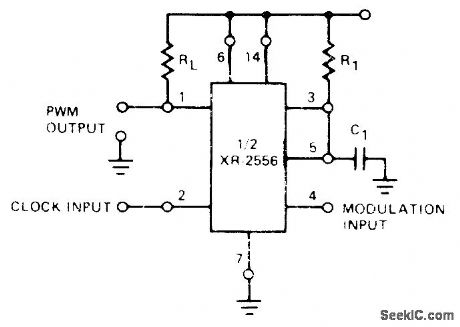
Half of Exar XR-2556 dual timer is connected to operate in monostable mode, for triggering with continuous pulse train. Output pulses are generated at same rate as input, with pulse duration determined by R1 and C1 Supply voltage is 4.5-16 V.- Timer Data Book, Exar Integrated Systems, Sunnyvale, CA, 1978, p 23-30. (View)
View full Circuit Diagram | Comments | Reading(1104)
THREE_WAVEFORM
Published:2009/7/6 22:12:00 Author:May
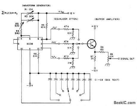
Gives simultaneous sine, square, and triangle outputs with low distortion (1%), high linearity (0.1%), 0.05 Hz to1 MHz frequency range, and duty cycle of 2% to 98%. Intersil 8038 waveform generator feeds buffer amplifier using 2N3709 transistor, switched to desired output waveform. Timing capacitors C1-C8, determining frequency decades of signal generator, start with 500,μF for 0.05 Hz to 0.5 Hz and decrease in submultiples of 10 to 500 pF for 50 kHz to 500 kHz. C8 is 250 pF for final range of 100 kHz to 1 MHz.-H. P.Fisher, Precision Waveform Generator, 73 Magazine, Dec. 1973, p 41-43. (View)
View full Circuit Diagram | Comments | Reading(2496)
4_digit_7_function_stopwatch_timer
Published:2009/7/21 23:27:00 Author:Jessie
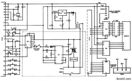
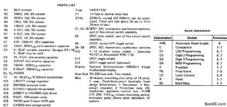
4-digit 7-function stopwatch/timer. See table for switch abbreviations. See parts list for component part numbers and values. This circuit is based on the MM5865 universal timer IC. As drawn the display resolution is 1 second. A SPST switch can be included between pin 16 of IC2 and Vss to provide a resolution of 0.01 second and 1 second. Another option is the display control switch which may be used to inhibit the display (courtesy National Semiconductor Corporation). (View)
View full Circuit Diagram | Comments | Reading(2028)
Application circuit example of transistor switch stabilized voltage supply
Published:2011/4/23 4:16:00 Author:May | Keyword: transistor switch, stabilized voltage supply
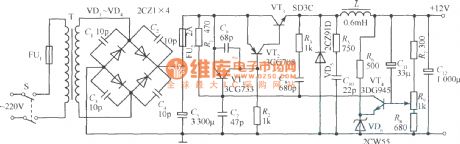
The application of transistor switch stabilized voltage supply is rather widespread. The diagram is a specific circuit example.
In the diagram, transformer T, diode VD1~VD4 and capacitor C5 make up rectifying and wave-filtering circuit; sampling circuit is series by resistor R7, R8 and potentiometer R9;transistor Vr4 is error amplifier; switch adjuster is complex consisting of transistor Vr2, Vr3; Vt1 is pulse width adjuster; self oscillation circuit consists ofVT1, VT2, VT3 and R3, C3; reference voltage source consists of resistor R6 and constant voltage diode; VD5 is fly-wheel diode; L is energy storage induction; output filter consists of VD5, L and C12; the loop composed of R5 and C10 can make fly-wheel diode having better restitution property.
Bridge rectifier outputs DC voltage after breaking over AC network source switch S. Its positive end is connected with emitter of VT2 tube. Its negative end offers bias to Vr2 by resistor R2. It can make complex switch adjuster saturation and breaking over. Output current can generate induced voltage which the left is positive and the right is negative when it is passing energy storage induction L.
(View)
View full Circuit Diagram | Comments | Reading(848)
LIGHT_BEAM_MODULATOR
Published:2009/7/6 22:11:00 Author:May
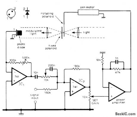
Intensity of light beam is modulated by rotating Polaroid vane driven by small motor. Since amplitude is not constant with change in frequency between 10 and 100 Hz, compensation is provided by sampling modulated beam with silicon photodiode that is linearized by IC1. Input and feedback signals are mixed by summing amplifier IC2, which drives noninverting power amplifier consisting of 741 opamp driving two OC28 power transistors connected in closed feedback loop having gain of 5. Power amplifier drives pen motor of modulator.-R. F. Cartwright, Constant Amplitude Light Modulator, Wireless World, Sept.1976, p 73. (View)
View full Circuit Diagram | Comments | Reading(644)
On_off_temperature_control_with_delayed_turn_on
Published:2009/7/21 23:26:00 Author:Jessie
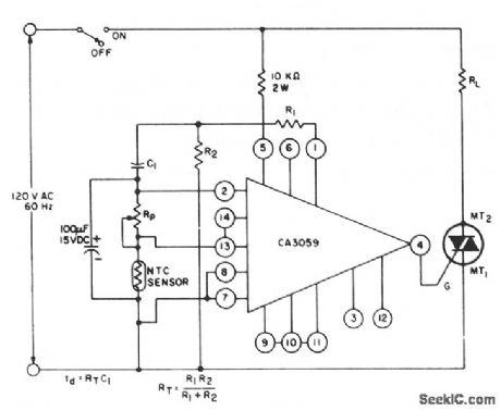
This circuit uses a CA3059 zero-voltage switch to control operation of atriac. The delay between switch closure and turn-on is set by the values of R1, R2 and C1 as shown by the equations. (View)
View full Circuit Diagram | Comments | Reading(1350)
SIMPLE_TWO_TONE_GENERATOR
Published:2009/7/6 22:11:00 Author:May

Circuit Notes
Two 741 operational amplifiers are used for the active element in this Wien bridge oscillator.(The 1458 is the dual version of the 741.) Frequencies of the two oscillators were chosen to fit standard component values. Other frequencies between 500 and 2000 Hz can be employed. They should not be harmonically related. The output level of U1A is set by a resistive divider, while the output of U1B is adjustable through R1. The output of the two oscillators is combined in U2, an op-amp adder with unity gain. The output from U2 can be adjusted using R2. (View)
View full Circuit Diagram | Comments | Reading(890)
Line_operated_thyristor_control_time_delay
Published:2009/7/21 23:24:00 Author:Jessie
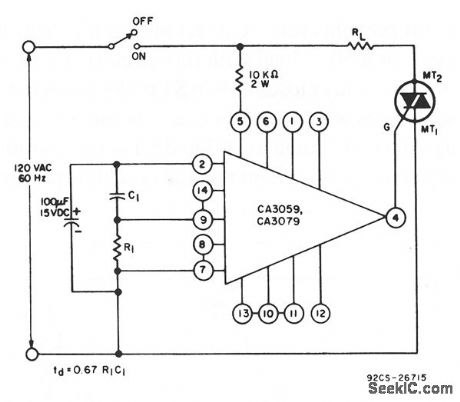
This circuit uses a CA3059 or CA3079 zero-voltage switch to control turn-on time of a triac. The delay between switch closure and turn-on is set by the values of R and C, as shown by the equation. (View)
View full Circuit Diagram | Comments | Reading(1077)
VEGATIVE_RAMP_
Published:2009/7/6 22:08:00 Author:May
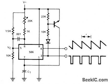
Connection shown for 566 function generator gives negative output ramp having period equal to 1/2f where f is normal free-running frequency of 566 as determined by supply voltage and RC values used. Ramp has very fast reset because PNP transistor charges timing capacitor C1 rapidly at end of discharge period. Short output pulse is available at pin 3.- Signetics Analog Data Manual, Signetics, Sunnyvale, CA, 1977, p 851. (View)
View full Circuit Diagram | Comments | Reading(1633)
DOUBLE_SIDEBAND_AM
Published:2009/7/6 22:07:00 Author:May
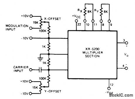
Connection shown for multiplier section of Exar XR-S200 PLL IC gives double-sideband AM output. X-offset adjustment for modulation input sets carrier out-put level, and Y-offset adiustment of carrier input controls symmetry of output waveform .Modulation input can also be used as linear automatic gain control (AGC)for controlling amplification with respect to carrier input signals, - Phase- Looked Loop Data Book, Exar Integrated Systems, Sunnyvale, CA, 1978, p9-16. (View)
View full Circuit Diagram | Comments | Reading(1048)
FIRE_SIREN
Published:2009/7/21 23:23:00 Author:Jessie

Pressing button produces rapidly rising wail, and releasing button gives slower lowering of frequency resembling sounds of typical siren on fire engine. Circuit uses National LM3909 IC operating from 1.5-V cell for driving 25-ohm loudspeaker, 1-μF capacitor and 200-ohm resistor determine width of loudspeaker pulse, while 2.7K resistor and 500-μF capacitor determine repetition rate of pulses.- Linear Applications, Vol. 2, National Semiconductor, Santa Clara, CA, 1976, AN-154, p 6-7. (View)
View full Circuit Diagram | Comments | Reading(1)
ONE_IC_AUDIO_GENERATOR
Published:2009/7/6 22:06:00 Author:May

Circuit NotesThis high-quality low-cost generator covers 20 Hz to 20 kHz in three bands with less than 1% distortion. LM1-10 V, 14 mA (344, 1869, 914) or 10 \/, 10 mA (913, 367).
A = oscillatorB = power Supply (View)
View full Circuit Diagram | Comments | Reading(647)
19MHz_universal_counter_using_an_Intersil_ICM7226B_40_pin_DIP
Published:2009/7/21 23:22:00 Author:Jessie
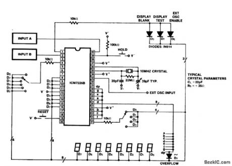
19MHz universal counter using an Intersil ICM7226B 40-pin DIP. This circuit measures frequencies at input A up to 10 MHz and at input B up to 2 MHz (courtesy Intersil, Inc.). (View)
View full Circuit Diagram | Comments | Reading(831)
| Pages:1013/2234 At 2010011002100310041005100610071008100910101011101210131014101510161017101810191020Under 20 |
Circuit Categories
power supply circuit
Amplifier Circuit
Basic Circuit
LED and Light Circuit
Sensor Circuit
Signal Processing
Electrical Equipment Circuit
Control Circuit
Remote Control Circuit
A/D-D/A Converter Circuit
Audio Circuit
Measuring and Test Circuit
Communication Circuit
Computer-Related Circuit
555 Circuit
Automotive Circuit
Repairing Circuit