
Index 86
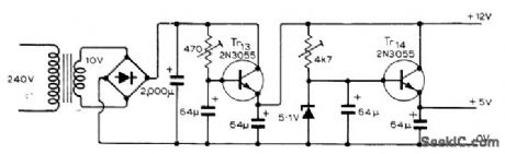
DUAL_5_V
Published:2009/7/16 22:10:00 Author:Jessie

Provides two 5-V regulated supplies for frequency counter, operating either from 9-VDC outputs of AC supply or from 12-VDC auto battery. Splitting of supply divides current demand so regulators operate well below maximum ratings and provide decoupling between sections of load.-J. Pollock, Six Digit 50-MHz Frequency Counter, Ham Radio, Jan. 1976, p 18-22.
(View)
View full Circuit Diagram | Comments | Reading(897)
Transistor tracking regulated power supply circuit diagram
Published:2011/7/20 5:14:00 Author:nelly | Keyword: Transistor, tracking, regulated power supply

As shown in the figure, it is the transistor tracking regulated power supply circuit, the input voltage is ±24V, the output voltage is 0~+15V and 0~-15V, the maximum output current is 3A.
(View)
View full Circuit Diagram | Comments | Reading(3157)
±4_V_TO_±25_V
Published:2009/7/16 22:09:00 Author:Jessie

Arrangement permits varying both positive and negative regulated output voltages simultaneously with single control, with maximum load current of 400mA for both regulators. Positive supply controls negative slave regulator to provide tracking within 0.05 V at full output. Developed for use in lab to observe effect of varying supply voltages on circuits under development. -J. A. Agnew, Dual Power Supply Delivers Tracking Voltages, EDN Magazine, Oct.15, 1970, p 51. (View)
View full Circuit Diagram | Comments | Reading(1905)
RADAR_DETECTOR
Published:2009/7/16 22:09:00 Author:Jessie
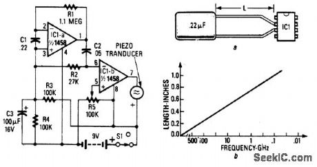
A simple detector of radar signals uses the junctions of the input transistors of an LM1458 op amp as RF detectors. The leads of C1 act as an antenna and should be about 0.4 long measured from the IC package. Detected audio components are further amplified by IC1A and IC1B, and drive a piezo transducer. Mount the circuit so that incident RF energy will not be blocked. (View)
View full Circuit Diagram | Comments | Reading(2937)
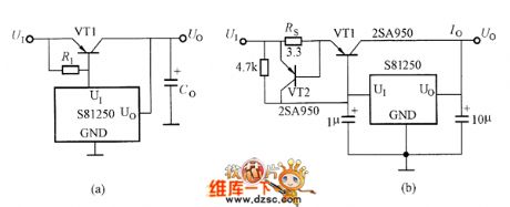
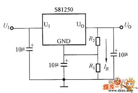
The application circuit diagram of S812/S802 series regulator
Published:2011/7/20 5:19:00 Author:nelly | Keyword: regulator
View full Circuit Diagram | Comments | Reading(799)
5_10_15_20_V_SWITCH
Published:2009/7/16 22:08:00 Author:Jessie
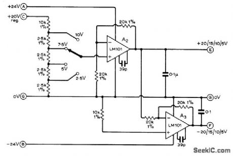
Reference voltage selected by switch is applied to noninverting input of opamp having voltage gain of 2, to provide both positive and negative regulated voltages at desired value, Any standard opamp, such as μA709 or μA741,can be used in place of National LM101.-T. D. Towers, Elements of Linear Microcircuits, Wireless World, July 1971, p 342-346. (View)
View full Circuit Diagram | Comments | Reading(613)
DELAYED_PULSE_GENERATOR
Published:2009/7/16 22:07:00 Author:Jessie

This circuit produces a delayed pulse width of 1.1(Rt2Ct2). The delay is given by T=1.1(Rt1Ct1). A 556 dual timer can be used. (View)
View full Circuit Diagram | Comments | Reading(4021)
Constant voltage and constant current regulated power supply circuit diagram
Published:2011/7/20 5:15:00 Author:nelly | Keyword: Constant voltage, constant current, regulated power supply

View full Circuit Diagram | Comments | Reading(5277)
ELECTROMAGNETIC_LEVITATOR
Published:2009/7/16 22:04:00 Author:Jessie
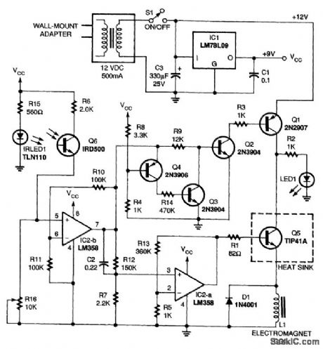
This circuit is used to levitate a steel ball as a demonstration of levitation via an electromagnet. An infrared photodetector is used to sense the position of a steel ball and control the current in the electromagnet via a feedback loop. An infrared emitter and detector mounted across from each other create an invisible beam that passes slightly below the coil. As the object rises toward the electro-magnet, it begins to block the beam. When the beam becomes blocked, the output of the detector is reduced, which, in turn, reduces the current in the electromagnet's coil. The reduced current weakens the magnetic field, the object begins to drop, and the detector once again sees more of the beam.This causes the circuit to increase the magnetic field, and the cycle repeats as the object is attracted upward again. The circuit is designed go that eventually an equilibrium is reached where the magnetic attraction exactly balances the force of gravity pulling on the object. The object then remains perfectly suspended in the infrared beam's path with no visible means of support! (View)
View full Circuit Diagram | Comments | Reading(1840)
KEYING_CIRCUIT
Published:2009/7/16 22:02:00 Author:Jessie
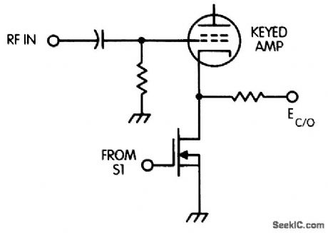
A power MOSFET can cathode-key a high-power RF amplifier. (View)
View full Circuit Diagram | Comments | Reading(658)
SPLIT_12_V_POWER_SUPPLY
Published:2009/7/16 22:01:00 Author:Jessie
Two IC regulators and a bridge circuit supply ±12 V. (View)
View full Circuit Diagram | Comments | Reading(2362)
DUAL_SUPPLY
Published:2009/7/16 22:00:00 Author:Jessie
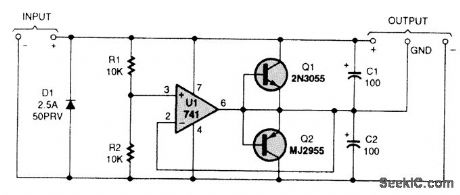
The key idea is that in a dual-supply powered circuit, ground is midway between the positive and negative supply voltages. Unfortunately, ordinary voltage regulators can't do the job. The reason is that they cart only source current, not sink it, and the ground terminal in a dual supply might have to either source or sink current, depending on which half of the load is drawing more current at the time. In the circuit, R1 and R2 divide the input voltage in half. Op amp U1 reproduces that voltage at the ground output terminal by making either Q1 or Q2 conduct as much as necessary. Capacitors Ct and C2 hold the output voltage steady when the load changes suddenly. Diode D1 is present to protect the circuit's input from reversed polarity by blowing the fuse of the main power supply. If your power supply has no fuse, place D1 in series with the circuit. That will afford the same protection with only slightly reduced regulation and voltage output. (View)
View full Circuit Diagram | Comments | Reading(1514)
INEXPENSIVE_PULSE_GENERATOR_FOR_LOGIC_TROUBLESHOOTING
Published:2009/7/16 21:58:00 Author:Jessie

Built around a 555 timer IC, this pulse generator can be built into a probe for logic troubleshooting. R11 is frequency controlled and gives a range of about 5 to 200 Hz. C2 can be reduced for higher frequencies. S2 selects one shot or pulse operators. Q1 and Q2 provide a fast rise-time pulse, which acts as a clipper amplifier. Q4 acts as a regulator. The supply can be anything from about 4.5 to 18 Vdc. LED1 is an indicator that shows circuit operation. (View)
View full Circuit Diagram | Comments | Reading(952)
12_V_FOR_TRANSCEIVER
Published:2009/7/16 21:58:00 Author:Jessie
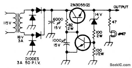
Permits operation of 144-MHz transceiver from AC line at base station. If 18-V transformer at 3 A is not available, use 12-V 3-A unit and add 26 turns No. 20 tefloncoated wire to secondary in proper phase. Choose transformer having enough room for these extra turns.-W. W. Pinner, Midland 2 Meter Base or Portable, 73 Magazine, Aug. 1974, p 61-63. (View)
View full Circuit Diagram | Comments | Reading(611)
NEON_TUBE_HIGH_VOLTAGE_POWER_SUPPLY
Published:2009/7/16 21:58:00 Author:Jessie
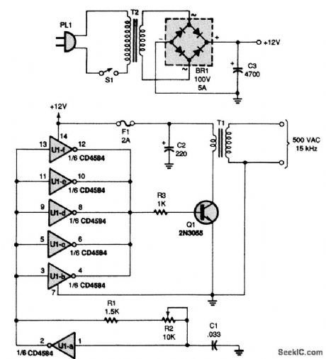
Power for the circuit is supplied by a step-down transformer (T2) and a full-wave bridge rectifier (BR1), which convert 117-Vac to 12-Vdc. Capacitor C3 acts as a filter. The heart of the circuit is a Schmitt-trigger hex inverter, U1. Capacitor C1, resistor R1, and potentiometer R2 are connected to one section of the inverter, U1-a, to form an oscillator that runs at approximately 15 kHz (because U1 is a Schmitt trigger, the output square wave is very clean). Adjusting R2 varies the frequency. The output of the oscillator is fed into the remaining five inverters (U1-b through U1-f), which are connected in parallel to create a buffer that is capable of increasing the drive current of the oscillator. The square-wave output is used to drive the switching transistor (Q1), which, in turn, switches the primary windings of the ferrite-core transformer (T1). Approximately 500-Vac at 15 kHz are output from the secondary of the transformer. T1 is made from a ferrite pot core. Wind 500 turns of #30-gauge wire for the secondary. Coat it with insulating varnish and add a layer of insulating tape, over which a 20-turn winding of #22 wire is wound to form the primary winding. (View)
View full Circuit Diagram | Comments | Reading(2076)
IMPROVED_CLIPPING_CIRCUIT_DESIGN
Published:2009/7/16 21:58:00 Author:Jessie
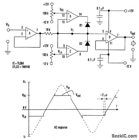
Op amps A and D form unity-gain buffer amplifiers. Op amps B and C compare the input voltage (Vin) with the reference voltages (VHi and VLo). These references set the high and low clipping levels of the circuit. When the input voltage lies in the range (VHi-VLo), the outputs of the comparators make both diodes (D1 and D2) reverse-biased. As a result, the circuit's output Vout follows the input voltage. When the input voltage exceeds the value VHi op amp B's output goes negative, forward-biasing D1 and thus reducing V1 the voltage at the invertinginput of op amp B. The circuit reaches an equilibrium condition at which Vout=V1=VHi Similarly, when the input voltage goes below the value VLo, op amp C's output goes positive, forward-biasing D2. This increases the voltage at V1, At the equilibrium condition, Vout=V1=VLo. The circuit's output continues to follow the input for about 2μs, even after the input voltage crosses the reference voltages, because of the slew rates of the op amps.The supplies (5V≤V+≤15V, -5V≥V-≥-15 V). (View)
View full Circuit Diagram | Comments | Reading(1259)
12_AND_5_V
Published:2009/7/16 21:57:00 Author:Jessie
Used with multiple photographic development timer to provide 12 V at about 5mA and 5 V at about 300mA for logic, control, and audible alarm circuits.-R. G. Wicker, Photographic Development Timer, Wireless World, April 1974, p 87-90. (View)
View full Circuit Diagram | Comments | Reading(561)
HV_POWER_SUPPLY
Published:2009/7/16 21:56:00 Author:Jessie
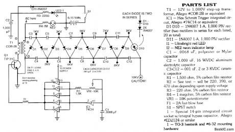
This power supply uses a Cockcroft-Walton HV multiplier circuit to produce up to 10 kV from a 12-V source. Up to 5 W is available from this circuit. (View)
View full Circuit Diagram | Comments | Reading(2194)
S812/S802 series adjustable regulator output voltage circuit diagram
Published:2011/7/20 5:18:00 Author:nelly | Keyword: regulator, output voltage
View full Circuit Diagram | Comments | Reading(1233)
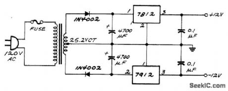
±6_V_AND_±12_V
Published:2009/7/16 21:56:00 Author:Jessie

Provides regulated power required by 5-MHz frequency standard and its temperature-controlled crystal oven. Current is measured by switching milliammeter and series resistor across current-limiting resistors R3 and R10, which also serve as meter shunts. DC input voltage at terminal 3 of MC1460R regulator should be at least 3 V greater than output voltage but should not exceed 20-V rating. Adjust R5 and R12 as required to get correct output voltages. Diodes ale 200 PIY at 0.5 A. T1 and T2 have 117-V primary and 25.2-V secondary at 0.3 A, T3 has 117-V primary and 6.3-V secondary at 1 A.-R. Silberstein, An Experimental Frequency Standard Using ICs, QST, Sept. 1974, p 14-21 and 167. (View)
View full Circuit Diagram | Comments | Reading(797)
| Pages:86/291 At 2081828384858687888990919293949596979899100Under 20 |
Circuit Categories
power supply circuit
Amplifier Circuit
Basic Circuit
LED and Light Circuit
Sensor Circuit
Signal Processing
Electrical Equipment Circuit
Control Circuit
Remote Control Circuit
A/D-D/A Converter Circuit
Audio Circuit
Measuring and Test Circuit
Communication Circuit
Computer-Related Circuit
555 Circuit
Automotive Circuit
Repairing Circuit