
Index 79
20_METER_DIRECT_CONVERSION_CW_SSB
Published:2009/7/16 4:53:00 Author:Jessie
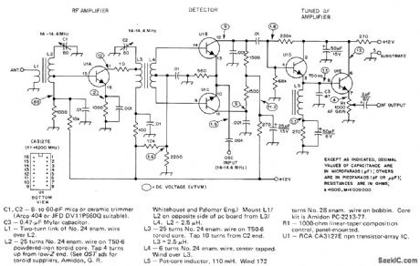
Simple direct-conversion or synchrodyne receiver uses RCA CA3127E five-transistor array. Product detector follows 14-MHz RF stage. Low drain makes receiver ideal for battery operation, but circuit has no AGC. AF output will drive headphones adequately for strong 20-meter signals, but not loudspeaker. Local-oscillator energy at 14-14.4 MHz for product detector at 1.5-2 VRMS must be furnished by external BFO.-D. DeMaw, Understanding Linear ICs, QST Jan. 1977, p 11-15. (View)
View full Circuit Diagram | Comments | Reading(2041)
SERIES_NPN_BASIC_LOGIC
Published:2009/7/16 4:53:00 Author:Jessie
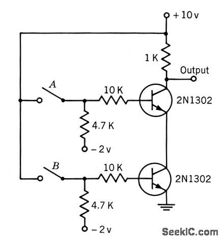
Serves as and gate for normally open switches, and as or gate for normally dosed switches. Provides phase inversion of input.-Texas Instruments Inc., Transistor Circuit Design, McGraw-Hill, N.Y., 1963, p 388. (View)
View full Circuit Diagram | Comments | Reading(703)
VARIABLE_PULSE_WIDTH_GENERATOR
Published:2009/7/16 4:51:00 Author:Jessie
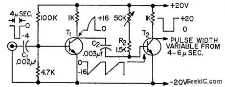
Converts fixed negative pulse-width input to variable and stable pulse width. Will accept positive inputs if T1 and T2 are changed from 2N1308 to 2N1309 and collector voltages reversed. Will operate at repetition rates from 30 cps to 2 Mc, with pulse widths from 600 microsec to 100 nsec. With values shown, maximum duty cycle is 92% with 63-microsec input rep rate.-H. D. Flagle, High-Duty-Cycle Pulse-Width Genera. tor, FEE, 11:8, p 27-28. (View)
View full Circuit Diagram | Comments | Reading(765)
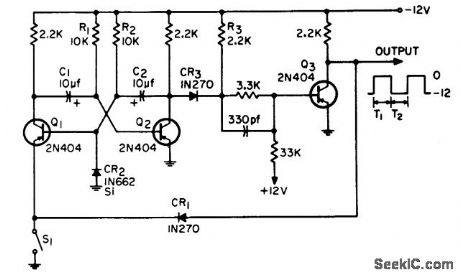
VARIABLE_FREQUENCY_AND_VARIABLE_DUTY_CYCLE
Published:2009/7/16 4:48:00 Author:Jessie
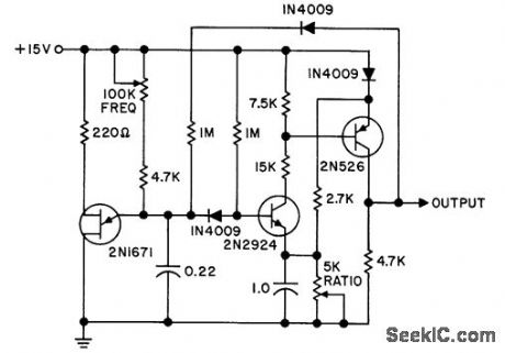
Frequency and duty ratio can be varied independently to generate desired rectangular wave. Uit is used in conventional sawtooth generator. Two transistors provide positive going output when uit emitter voltage exceeds npn emitter voltage. Frequency range is 60 to 1,000 cps.- Transistor Manual, Seventh Edition, General Electric Co. 1964, p 344. (View)
View full Circuit Diagram | Comments | Reading(1100)
POWERED_SUBWOOFER
Published:2009/7/13 2:18:00 Author:May

The power supply consists of a center-tapped 48-V transformer, a bridge rectifier, and filter capacitors. The rectified and filtered output is about ±35 V. The power supply for op amp IC1 is regulated to ±15 V by zener diodes D1 and D2 and resistors R19 and R20. The input circuit consists of a mixer and voltage divider formed by resistors R1 and R2, potentiometer R3, and unity-gain buffer IC1-a. Potentiometer R3 is provided to adjust the output of the subwoofer to the desired level. Op amp IC1-b provides a 12-dB-peroctave high-pass filter with capacitors C2 and C3 and resistors R5 and R6. The cutoff frequency for this filter is 1/2πRC, or about 34 Hz with the values shown. Resistors R8 and R7 set the gain and Q of the filter. Capacitor C1 and resistor R4 form an additional 6-dB-peroctave high-pass filter at about 20 Hz. A 12-dB-peroctave low-pass filter is formed by IC1-c, C4 and C5, and R9 and R10. The values shown set the low-pass cutoff at 72 Hz. The gain and Q of this stage are set by R11 and R12. These two filters, connected back-to-back, form a bandpass filter. When operated with ±15-V supplies, the output of op amp IC1-d can swing about 10 V peak to drive transistors Q1 and Q2. Resistors R17 and R18 provide negative feedback, and set the gain of the out-put stage at about 3. Hence, the output can swing to about 30 V peak. As long as the transistors are the high-beta types specified, the peak power output into an 8-Ω load is (30×30/8)/2556 W rms. The overall gain of the amplifier is set by resistor R13 and feedback resistor R14. (View)
View full Circuit Diagram | Comments | Reading(5099)
CURRENT_DIFFERENCE_AMPLIFIER_USAGE_CIRCUITS
Published:2009/7/13 2:15:00 Author:May
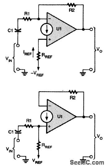
Here a current difference amplifier is used much like an op amp in an inverting follower circuit.Here is a noninverting follower built around a current difference amplifier. (View)
View full Circuit Diagram | Comments | Reading(554)
2500V_AT_500_mA
Published:2009/7/13 2:15:00 Author:May
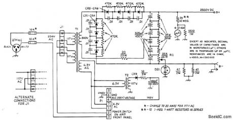
Meets power requirements for 2-kW linear amplifier using pair of 8873 conduction-cooled triodes fol SSB transmitter service. Power transformer is Hammond 101165.Diodes are 1000 PIY at 2.5A,such as Motorola HEP170.T2 is Stancor P-8190 rated 6.3 V at 1.2A.DS1 is 117-V neon pilot lamp Set tap on R1 5000 ohms from B-lead Make adjustments only after tuming off power and allowing time for capacitors to discharge; output voltages are dangerous.-R. M. Myers and G. Wilson, 8873s in a Two-Kilowatt Amplifier, QSL Oct. 1973, p 14-19.
(View)
View full Circuit Diagram | Comments | Reading(1234)
Adjustable regulated power supply circuit with heavy current
Published:2011/7/19 10:04:00 Author:Nancy | Keyword: Adjustable regulated power supply, heavy current
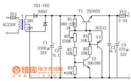
The regulated power supply is adjustable between the range of 3.5V to 25V, the current is heavy and it adopts adjustable regulating transistor circuit to obtain satisfied and stable voltage.
Working principle: The DC voltage is provided to the base of regulating transistor by R1 after filtered and rectified, which makes regulating transistor conduct, and when V1 conducts, the voltage across RP, R2 make V2 conduct. The emitter and collector voltage of V1,V2 and V3 don't change any longer (the function is as same as the regulating transistor). You can obtain stable output voltage by adjusting RP, the ratio of R1, RP, R2 and R3 decides the value of output voltage of the circuit. (View)
View full Circuit Diagram | Comments | Reading(2212)
Adjustable regulated power supply circuit with overload and short circuit protection function
Published:2011/7/19 9:46:00 Author:Nancy | Keyword: Adjustable regulated power supply, overload, short circuit protection
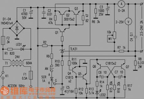
The circuit has the overload, short circuit protection and alarm function. Under the overload condition, the voltage drop of the resistor R8 increases. When the voltage drop reaches 0.6V, SCR conducts, which makes the Q1 base electric potential drop to about 1V, so the transistor Q1 and the regulating transistor Q2, Q3 cut off to protect regulating transistor from burning out. After Q2 and Q3 cut off, the output voltage is zero and the electronic switch Q4 cut off, Q5 conducts, which make the multivibrator composed by Q6 and Q7 start oscillation (dozens of Hertz), light-emitting diode LED2 flashes to alarm. (View)
View full Circuit Diagram | Comments | Reading(2064)
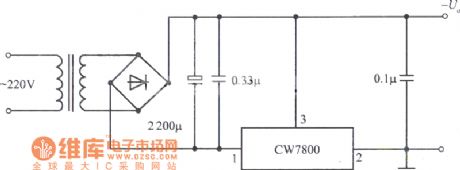
Integrated regulated voltage supply basic circuit with fixed output
Published:2011/7/19 9:25:00 Author:Nancy | Keyword: fixed output, integrated regulated voltage supply
View full Circuit Diagram | Comments | Reading(523)
500_W_AT_20_kHz
Published:2009/7/13 1:49:00 Author:May
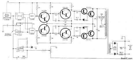
Uses four Delco DTS-712 transistors in push-pull Darlington configuration, with pulse-width modulation on push-pull inverter providing regulation. Can be operated from 220-VAC three-phase full-wave rectified line. Efficiency is up to 80%. Square-wave output of 40-kHz primary oscillator drives JK flipflop that generates complementary square waves and divides frequency by 2 with necessary symmetry. NAND gates establish primary ON/OFF periods of power stage. Portion of output signal is compared to reference voltage, and error signal is fed to NAND gates to give regulation better than 0.1% for load range of 200-500 W or line range of 300-400 V.- A 20 kHz, 500 W Regulating Converter Using DTS-712 Transistors, Delco, Kokomo, IN, 1974, Application Note 55. (View)
View full Circuit Diagram | Comments | Reading(1770)
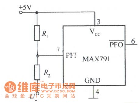
monitoring negative power supply circuit
Published:2011/7/19 10:05:00 Author:Nancy | Keyword: negative power supply
View full Circuit Diagram | Comments | Reading(538)
NEGATIVE_SUPPLY_GENERATOR
Published:2009/7/16 20:49:00 Author:Jessie
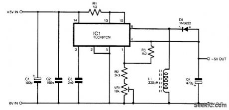
The TLC497CN is very useful for applications that do not involve high output currents. It provides a cost-effective means of providing a negative supply of up to about 150 mA. A circuit diagram for an inverter based on this device is shown. The efficiency of the circuit is typically a little over 50 percent with an input potential of 10 V, but is significantly under 50 percent with an input supply of 5 V. Capacitors C1 and C2 are supply-decoupling components on the input supply. Resistor R1 is the series resistance in the current-limiting circuit at the input to IC1. This is an essential safety feature because the circuit will Often be fed from a high-current supply that could almost instantly fry IC1 in the event of an overload on the device's output. Capacitor C3 is the timing component in the oscillator section of the PWM. The TLC497CN uses a fixed pulse width and a variable clock frequency to control the average output voltage. (View)
View full Circuit Diagram | Comments | Reading(782)
RASTER_VERTICAL_SWEEP
Published:2009/7/16 20:49:00 Author:Jessie

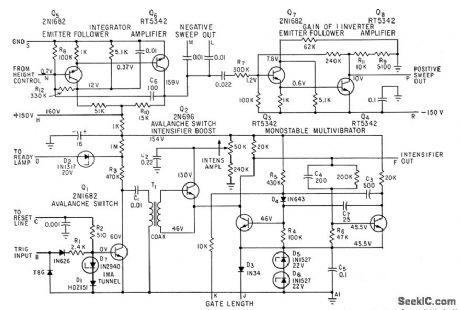
Q1 in shaper triggers intensifier pulse for test oscilloscope using tv type scanning, while remainder of circuit generates vertical sweep for scope used to measure time intervals in range of 0.5 to 100 microsec with time resolution of 0.05 microsec.-R.P.Rufer and W. A. Karlotski, Use Raster Oscilloscopes for Faster time Measurements, Electronics, 35:52, p 38-42. (View)
View full Circuit Diagram | Comments | Reading(1244)
0_to_±35_V
Published:2009/7/16 20:49:00 Author:Jessie
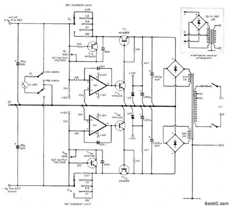
Twin stabilized DC supply uses ganged pots R1and R1a to set both positive and negative regulated outputs at any desired value up to 35 V. Input supplies from bridge rectifiers also provide ±12 V lines for 741 opamps. Load regulation is within 2 mV from no load to full 2-A maximum output. Output hum, noise, and ripple are together only 150 μV and independent of load.-J. L. Linsley Hood, Twin Voltage Stabilized Power Supply, Wireless world. Jan.1975, p 43-45.
(View)
View full Circuit Diagram | Comments | Reading(1616)
STEP_DOWN_REGULATOR
Published:2009/7/16 20:48:00 Author:Jessie

There are several versions of the LM2575T. The device used here has an ADJ suffix, which indicates that it has an adjustable output voltage. Pin 4 connects to the inverting input of the internal error amplifier. This amplifier's noninverting input is fed from a 1.2-V reference source. A discrete potentiometer connected across the output and feeding into pin 4 enabling the output voltage to be set at any figure above 1.2 V. In this case, the potentiometer is formed by VR1 in series with resistor R1. The adjustment range provided by VR1 is from 1.2 V to a little over 16 V. Higher output voltages can be accommodated by making R1 lower in value, but a circuit of this type is mainly used where there is a large voltage difference between the input and the output. Consequently, it is unlikely to be used with output voltages of more than about 16 V. The absolute maximum input voltage is 40 V. (View)
View full Circuit Diagram | Comments | Reading(2158)
GATED_ASTABLE_PULSE_TRAIN_GENERATOR
Published:2009/7/16 20:47:00 Author:Jessie
Uses standard logic circuits with self-completing action to produce pulse train having any desired integral number of pulses. First pulse starts when S1 is closed, and last pulse is completed when S1 is open. Selfcompleting action is produced by or function of S1 und CR1.-M. Neidich, Self-Completing Gated Astable, EEE, 13:1, p 66 and 75. (View)
View full Circuit Diagram | Comments | Reading(887)
NE602_DC_SUPPLY_INTERFACE
Published:2009/7/16 20:47:00 Author:Jessie
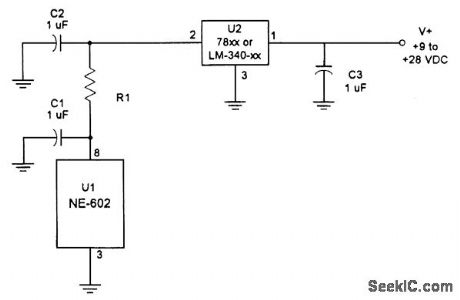
This is one method of deriving the 4.5-to 8.0-Vdc supply needed by the NE602 chip. (View)
View full Circuit Diagram | Comments | Reading(647)
STEP_UP_REGULATOR
Published:2009/7/16 20:46:00 Author:Jessie
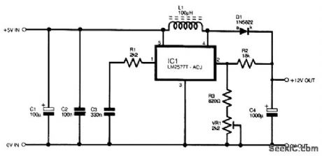
Refer to the figure for the circuit diagram of the step-up regulator. This circuit is based on an LM2577T-ADJ, which is designed to give a combination of high performance and simplicity. It can provide output currents of up to 3 A, and it has both overcurrent and thermal-protection circuits built in. It requires a minimum input potential of 3.5 V, and it shuts down automatically if the input voltage is inadequate. The maximum input voltage is 40 V. Capacitors C1 and C2 provide supply decoupling at the input, and C3 and resistor R1 provide frequency compensation. Inductor L1, diode D1, and an internal switching transistor of IC1 form a standard step-up output stage, with output smoothing provided by capacitor C4. Resistors R2 and R3 and preset VR1 form a potential divider that controls the output voltage. IC1 has an internal 1.2-V reference generator, and the voltage at pin 2 is, therefore, stabilized at this figure. With the specified values in the potential divider circuit, the output voltage range is around 9.5 to 25 V. (View)
View full Circuit Diagram | Comments | Reading(2093)
BASIC_BUCK_CONVERTER_CIRCUIT
Published:2009/7/16 20:45:00 Author:Jessie

The buck regulator is an alternative single-transistor converter. Series transistor Q1 chops the input voltage and applies the pulse to an averaging inductive-capacitive filter, consisting of L1 and C1.The output voltage of this simple filter is lower than its input voltage. (View)
View full Circuit Diagram | Comments | Reading(840)
| Pages:79/291 At 206162636465666768697071727374757677787980Under 20 |
Circuit Categories
power supply circuit
Amplifier Circuit
Basic Circuit
LED and Light Circuit
Sensor Circuit
Signal Processing
Electrical Equipment Circuit
Control Circuit
Remote Control Circuit
A/D-D/A Converter Circuit
Audio Circuit
Measuring and Test Circuit
Communication Circuit
Computer-Related Circuit
555 Circuit
Automotive Circuit
Repairing Circuit