
Audio Circuit
Index 30
Linear_FM_detector
Published:2009/7/24 23:43:00 Author:Jessie
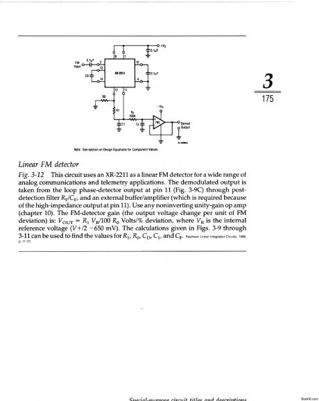
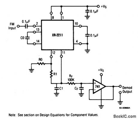
This circuit uses an XR-2211 as a linear FM detector for a wide range of analog communications and telemetry applications. The demodulated output is taken from the loop phase-detector output at pin 11 (Fig. 3-9C) through post-detection filter RF/CF, and an external buffer/amplifier (which is required because of the high-impedance output at pin 11). Use any noninverting unity-gain op amp (chapter 10). The FM-detector gain (the output voltage change per unit of FM deviation) is: VOUT=R1 VR/100 R0 Volts/% deviation, where VR is the internal reference voltage (V+/2 -650 mV). The calculations given in Figs. 3-9 through 3-11 can be used to find the values for R1, R0, CD, C1, and CF. (View)
View full Circuit Diagram | Comments | Reading(2137)
AUDIO_CONTINUITY_TESTER
Published:2009/6/26 4:05:00 Author:Jessie
This low-current audio continuity tester indicates the unknown resistance value by the frequency of audio tone. A high tone indicates a low resistance, and a tone of a few pulses per second indicates a resistance as high as 30 megohms. (View)
View full Circuit Diagram | Comments | Reading(1812)
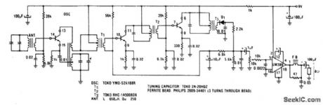
FM_RADIO
Published:2009/6/26 3:43:00 Author:May
View full Circuit Diagram | Comments | Reading(0)
AM_RADIO
Published:2009/6/26 3:39:00 Author:May
View full Circuit Diagram | Comments | Reading(4)
AM_FM_CLOCK_RADIO
Published:2009/6/26 3:38:00 Author:May
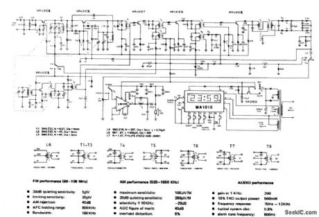
View full Circuit Diagram | Comments | Reading(814)
100_MHz_MIXER
Published:2009/6/25 21:34:00 Author:May
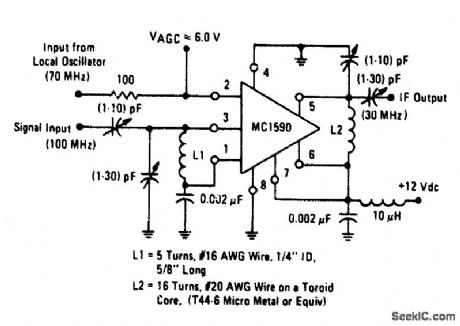
View full Circuit Diagram | Comments | Reading(2)
STEREO_BALANCE_METER
Published:2009/6/25 21:44:00 Author:Jessie
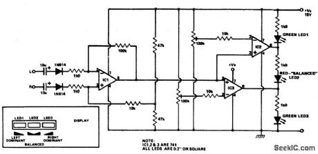
Outputs from each channel are fed to the two inputs of IC1 conrfected as a differential amplifier. IC2 and 3 are driven by the output of IC1. Output of IC1 is connected to the nonin-verting inputs of IC2 and 3. If the output of IC1 approaches the supply rail, the outputs of ICs 2 and 3 will also go high, illuminating LED3. This would happen if the right channel were dominating. If the left channel was dominant, the outputs of ICs 2 and 3 would be low, il-luminating LED1. If the two channels are equal in amplitude, the outputs of ICs 2 and 3 would be high and low respectively, lighting up LED2. (View)
View full Circuit Diagram | Comments | Reading(2968)
LOCAL_OSCILLATOR_FOR_DOUBLE_BALANCED_MIXERS
Published:2009/6/24 21:19:00 Author:May
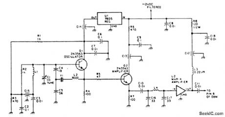
This circuit has an amplifier to supply +10 dBm to an SBL series (Mini-circuits) or similar type doubly-balanced mixer assembly. This circuit has values shown for =80- to 90-MHz crystals, although values of oscillator circuit constants can be scaled for higher or lower frequencies. (View)
View full Circuit Diagram | Comments | Reading(0)
SIMPLE_CRYSTAL_RADIO
Published:2009/6/24 4:27:00 Author:May
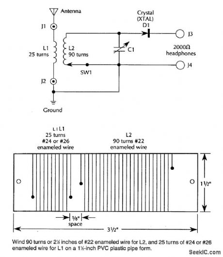
An IN34A (D1) is used as a detector in this crystal radio. A good outdoor antenna should be used. (View)
View full Circuit Diagram | Comments | Reading(0)
TWO_BAND_RADIO
Published:2009/6/24 4:25:00 Author:May
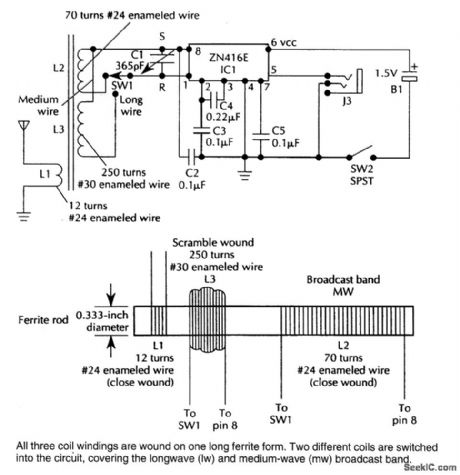
This TRF receiver covers the AM broadcast band and longwave bands (used in Europe and Asia for broadcasting). A loop antenna is used for reception and an extemal antenna can be connected.Frequency coverage is 150 to 1600 kHz. (View)
View full Circuit Diagram | Comments | Reading(0)
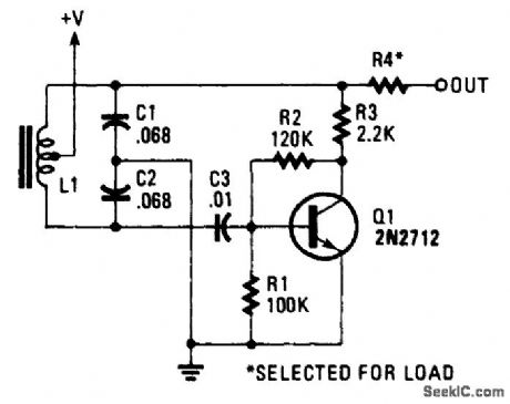
LC_AUDIO_OSCILLATOR
Published:2009/6/24 4:06:00 Author:Jessie
View full Circuit Diagram | Comments | Reading(1509)
TWO_POLE_FAST_TURN_ON_NAB_TAPE_PERAMPLIFIER
Published:2009/6/24 3:47:00 Author:Jessie
View full Circuit Diagram | Comments | Reading(649)
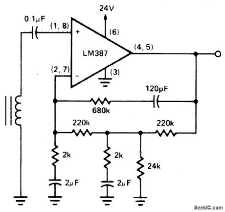
DISC_TAPE_PHASE_MODULATED_READBACK_SYSTEMS
Published:2009/6/24 3:44:00 Author:Jessie
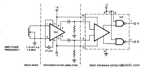
View full Circuit Diagram | Comments | Reading(1128)
TRANSFORME_RLESS_BALANCE_INPUTS_MICROPHONE_PREAMP
Published:2009/6/24 3:39:00 Author:Jessie
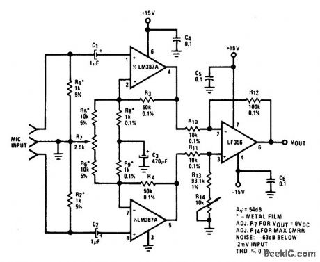
View full Circuit Diagram | Comments | Reading(0)
ULTRA_HIGH_GAIN_AUDIO_AMPLIFIER
Published:2009/6/24 3:33:00 Author:Jessie
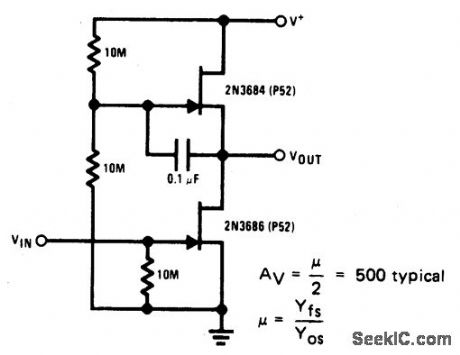
Sometimes called the JFET μt-amp, this circuit provides a very low power, high gain amplifying function. Since pt of a JFET in-creases as drain current decreases, the lower drain current is, the more gain you get. Input dynamic range is sacrificed with increasing gain, however. (View)
View full Circuit Diagram | Comments | Reading(0)
HIGH_SLEW_RATE_POWER_OP_AMP_AUDIO_AMP
Published:2009/6/24 3:24:00 Author:Jessie
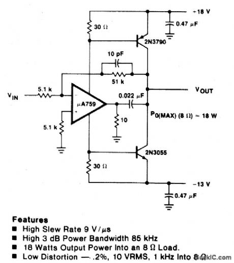
View full Circuit Diagram | Comments | Reading(0)
COMPLEX_SOUND_EFFECT_GENERATOR
Published:2009/6/24 2:38:00 Author:Jessie
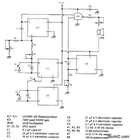
This system uses four free running oscillators to produce a wide variety of complex sounds. LF oscillator IC3 modulates IC2, which modulates IC1. The audio from IC1 is combined with a variable frequency from IC4. Switches at various points allow oscillators IC3 to be switched in or out, IC1 and IC2 to be varied in frequency, and IC4 also can be varied in frequency. The circuit is not critical and different arrangements can be tried to produce various sound effects. (View)
View full Circuit Diagram | Comments | Reading(0)
FOUR_CHANNEL_MIXER
Published:2009/6/24 2:23:00 Author:May
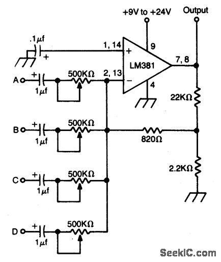
High gain op amp combines up to four individually controlled input signals. The dc power source should be well filtered (battery is ideal), and the circuit should be well shielded to prevent hum pickup. (View)
View full Circuit Diagram | Comments | Reading(2158)
HYBRID_MIXER
Published:2009/6/24 2:22:00 Author:May
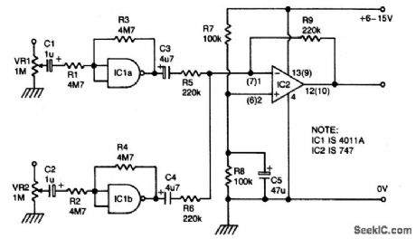
IC1a and b are biased into the linear regions by R3 and R4. (IC1 must be 4011A). Outputs from gates are combined by op amp IC2, which provides low impedance output. (View)
View full Circuit Diagram | Comments | Reading(815)
SILENT_AUDIO_SWITCHING_MIXING
Published:2009/6/24 2:21:00 Author:May
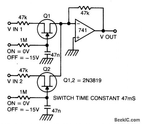
Two or more signals can be switched and/or mixed without annoying clicks by using FETs and a low input-impedance op amp circuit. (View)
View full Circuit Diagram | Comments | Reading(997)
| Pages:30/54 At 202122232425262728293031323334353637383940Under 20 |
Circuit Categories
power supply circuit
Amplifier Circuit
Basic Circuit
LED and Light Circuit
Sensor Circuit
Signal Processing
Electrical Equipment Circuit
Control Circuit
Remote Control Circuit
A/D-D/A Converter Circuit
Audio Circuit
Measuring and Test Circuit
Communication Circuit
Computer-Related Circuit
555 Circuit
Automotive Circuit
Repairing Circuit