BFG541, BFG541115, BFG55 Selling Leads, Datasheet
MFG:NXP Package Cooled:2009+ROHS D/C:19600

BFG541, BFG541115, BFG55 Datasheet download

Part Number: BFG541
MFG: NXP
Package Cooled: 2009+ROHS
D/C: 19600


MFG:NXP Package Cooled:2009+ROHS D/C:19600
BFG541, BFG541115, BFG55 Datasheet download
MFG: NXP
Package Cooled: 2009+ROHS
D/C: 19600

Want to post a buying lead? If you are not a member yet, please select the specific/related part number first and then fill the quantity and your contact details in the "Request for Quotation Form" on the left, and then click "Send RFQ".Your buying lead can then be posted, and the reliable suppliers will quote via our online message system or other channels soon.
TOP
PDF/DataSheet Download
Datasheet: BFG541
File Size: 144521 KB
Manufacturer: PHILIPS [Philips Semiconductors]
Download : Click here to Download
PDF/DataSheet Download
Datasheet: BFG10
File Size: 76569 KB
Manufacturer: PHILIPS [Philips Semiconductors]
Download : Click here to Download
PDF/DataSheet Download
Datasheet: BFG10
File Size: 76569 KB
Manufacturer: PHILIPS [Philips Semiconductors]
Download : Click here to Download
NPN silicon planar epitaxial transistor, intended for wideband applications in the GHz range, such as analog and digital cellular telephones, cordless telephones (CT1, CT2, DECT, etc.), radar detectors, satellite TV tuners (SATV), MATV/CATV amplifiers and repeater amplifiers in fibre-optic systems.
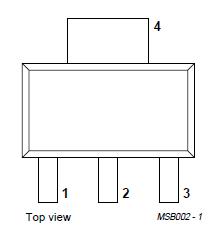
The transistors are mounted in a plastic SOT223 envelope.
| SYMBOL | PARAMETER | CONDITIONS |
MIN. |
TYP. |
MAX. |
UNIT |
| VCBO | collector-base voltage | open emitter |
- |
- |
20 |
V |
| VCES | collector-emitter voltage | RBE = 0 |
- |
- |
15 |
V |
| IC | DC collector current |
- |
- |
120 |
mA | |
| Ptot | total power dissipation | Ts 60 °C; note 1 |
- |
- |
650 |
mW |
| hFE | DC current gain | IC = 40 mA; VCE = 8 V; Tj = 25 °C |
100 |
120 |
250 |
|
| Cre | feedback capacitance | IC = 0; VCE = 8 V; f = 1 MHz |
- |
0.7 |
- |
pF |
| fT | transition frequency | IC = 40 mA; VCE = 8 V; f = 1 GHz; Tamb = 25 °C |
- |
9 |
- |
GHz |
| GUM | maximum unilateral power gain | IC = 40 mA; VCE = 8 V; f = 900 MHz; Tamb = 25 °C |
- |
15 |
- |
dB |
| IC = 40 mA; VCE = 8 V; f = 2 GHz; Tamb = 25 °C |
- |
9 |
- |
dB | ||
| |s21|2 | insertion power gain | IC = 40 mA; VCE = 8 V; f = 900 MHz; Tamb = 25 °C |
15 |
14 |
- |
dB |
| F | noise figure | Gs = Gopt; IC = 10 mA; VCE = 8 V; f = 900 MHz; Tamb = 25 °C |
- |
1.3 |
1.8 |
dB |
| PL1 | output power at 1 dB gain compression |
IC = 40 mA; VCE = 8 V; RL = 50 ; f = 900 MHz; Tamb = 25 °C |
- |
21 |
- |
dB |
| ITO | third order intercept point | IC = 40 mA; VCE = 8 V; RL = 50 ; f = 900 MHz; Tamb = 25 °C |
- |
34 |
- |
dB |

Price: 4-6 USD
MT58L64L18CT-10 TQFP100

Price: 5-6.5 USD
DL-7140-211M laser tube

Price: 4-5 USD
74LVC74APG - IC FLIP FLOP D-Type POS-EDG DUAL 14TSSOP

Price: 6.5-8 USD
CYPRESS - Clock Synthesizer with Differential CPU Outputs

Price: 0.284-0.286 USD
PI5V330QEX Pericom Multiplexer Switch ICs

Price: 1-2 USD
IGBT power module, Single switch, 1200 V, Collector-emitter voltage, 430A

Price: 1-2 USD
a-Si TFT-LCD, NEC, 228.096Hmm, 560V

Price: 0.124-0.2 USD
PC354N1T - Mini-flat Package, AC Input Type Photocoupler - Sharp Electrionic Components

Price: 0.177-0.178 USD
RL1210JR51-XX-BL - Thick Film Chip Resistor Low Ohmic - TAITRON Components Incorporated

Price: 0.053-0.055 USD
STPS140A - POWER SCHOTTKY RECTIFIER - STMicroelectronics

Price: 1.45-1.5 USD
STA013 - MPEG 2.5 LAYER III AUDIO DECODER - STMicroelectronics

Price: 0.073-0.075 USD
SMBJ5347B - 5 Watt Surface Mount Silicon Zener Diodes - Micro Commercial Components
