
Circuit Diagram
Index 7
Audi A6 Radio Schematic
Published:2014/4/20 20:42:00 Author:lynne | Keyword: Audi A6 Radio Schematic
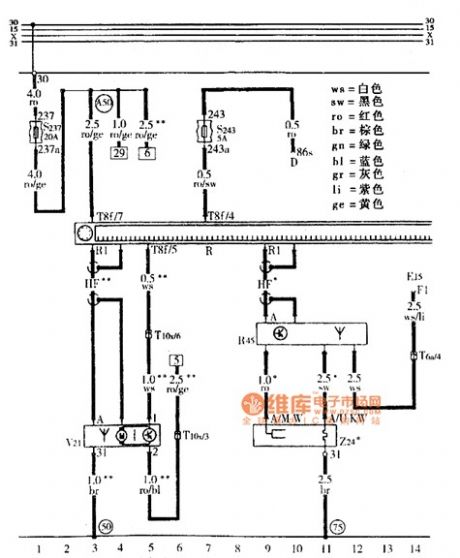
Audi A6 Radio Schematic shown as follow:
(View)
View full Circuit Diagram | Comments | Reading(2134)
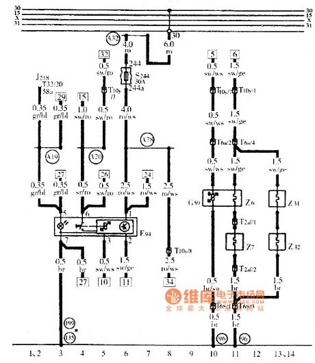
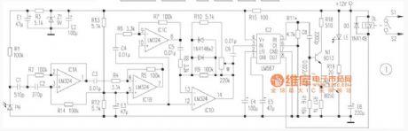
Air condition control circuit diagram
Published:2014/4/20 20:45:00 Author:lynne | Keyword: Air condition control circuit diagram
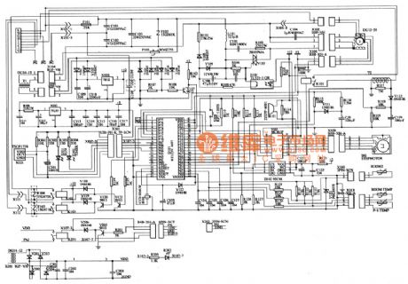
Air condition control circuit diagram as shown:
(View)
View full Circuit Diagram | Comments | Reading(1474)
Antenna circuit diagram
Published:2014/4/20 20:47:00 Author:lynne | Keyword: Antenna circuit diagram
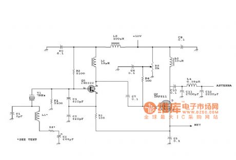
Antenna circuit diagram shown as follow:
(View)
View full Circuit Diagram | Comments | Reading(1794)
Ethernet interface circuit - DM9000 Network
Published:2014/4/20 20:49:00 Author:lynne | Keyword: Ethernet interface circuit - DM9000 Network, DM9000
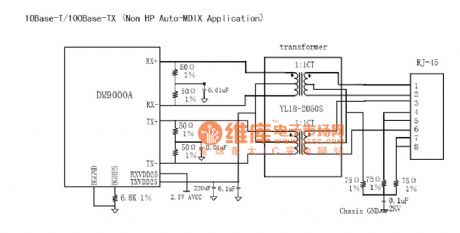
Ethernet interface circuit - DM9000 Network as shown:
(View)
View full Circuit Diagram | Comments | Reading(1540)
Ethernet interface circuit - CS8952 Network
Published:2014/4/20 21:17:00 Author:lynne | Keyword: CS8952
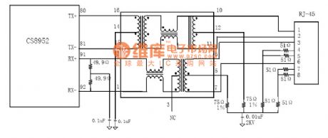
Ethernet interface circuit - CS8952 Network shown as follow:
(View)
View full Circuit Diagram | Comments | Reading(1304)
Power supply circuit diagrams
Published:2014/4/17 21:32:00 Author:lynne | Keyword: Power supply circuit diagrams
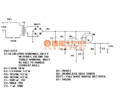
Power supply circuit diagram shown as follow:
(View)
View full Circuit Diagram | Comments | Reading(6070)
Audi A6 rear window electric shutter circuit diagram
Published:2014/4/17 21:31:00 Author:lynne | Keyword: Audi A6 rear window electric shutter circuit diagram
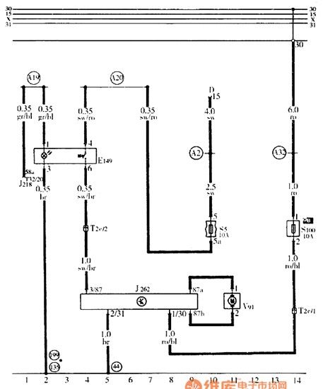
Audi A6 rear window electric shutter circuit diagram shown as follow:
(View)
View full Circuit Diagram | Comments | Reading(1374)
Audi A6 heated seats Circuit Diagram
Published:2014/4/17 21:29:00 Author:lynne | Keyword: Audi A6 heated seats Circuit Diagram
Audi A6 heated seats Circuit Diagram as shown:
(View)
View full Circuit Diagram | Comments | Reading(1446)
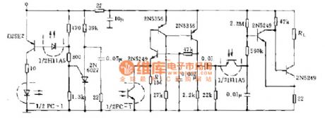
Infrared Circuit Schematic
Published:2014/4/17 21:28:00 Author:lynne | Keyword: Infrared Circuit Schematic
Infrared Circuit Schematic shown as follow:
(View)
View full Circuit Diagram | Comments | Reading(1455)
The LM76R pinout circuit diagram
Published:2014/4/17 21:26:00 Author:lynne | Keyword: The LM76R pinout circuit diagram, LM76R

LM76 is an integrated circuit by a digital temperature sensor, I2C serial bus interface and temperature window comparator composition. In the temperature range 70 ℃ ~ 100 ℃ and -10 ℃ ~ +45 ℃, the accuracy of its window comparator serial bus interface is ± 1 ℃. At 25 ℃, LM76CHM accuracy up to ± 0.5 ℃. Its open drain interrupt output (INT) when the temperature exceeds a programmable temperature window is activated, the temperature limit alarm output (T-CRIT-A) in the temperature exceeds a programmable limit the danger temperature (over temperature will damage LM76) valid.
(View)
View full Circuit Diagram | Comments | Reading(1149)
Infrared remote monitoring circuit schematics
Published:2014/4/16 20:47:00 Author:lynne | Keyword: Infrared remote monitoring circuit schematics
The circuit shown in Figure can be transmitted over a long distance signal detected target. PC1 infrared diode and phototransistor pair, when a target object or irradiating light barrier diode phototransistor, the phototransistor is turned on in the turned off, and through amplification and second infrared diode and phototransistor and power amplifier for transmission to the load (alarm or lights), the second of the infrared diode and phototransistor pair from the fail-safe action. Infrared remote monitoring circuit diagram shown in Figure:
(View)
View full Circuit Diagram | Comments | Reading(1291)
RF circuit diagram
Published:2014/4/16 20:46:00 Author:lynne | Keyword: RF circuit diagram
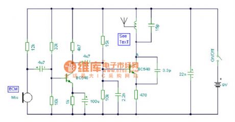
RF circuit diagram shown as follow:
(View)
View full Circuit Diagram | Comments | Reading(1461)
Lights Timing Flashing Circuit Diagram
Published:2014/4/16 20:45:00 Author:lynne | Keyword: Lights Timing Flashing Circuit Diagram, 2N5060, MPU131
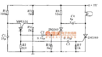
MPU131 thyristor is programmed with R1 and C1 class into relaxation oscillator circuit, the output control two-way thyristor 2N5060, thereby allowing low-voltage (2V) indicator lights timed flash.
(View)
View full Circuit Diagram | Comments | Reading(2176)
Signal repeater circuit schematic
Published:2014/4/16 20:40:00 Author:lynne | Keyword: Signal repeater circuit schematic, RC4558
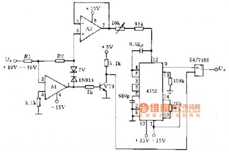
Illustrates the use of two operational amplifiers constituting the signal and a frequency-voltage converter A1.A2 transfer circuit 4153, the input signal UF amplitude varies between -10 ~-10V, the output signal UA, issued by the exclusive or gate. A1.A2 op amp can be used RC4558 or other models can be used 2N222 transistor VT1 or similar model, resistor R1 (10Ω) accuracy class shall be of ± 0.1%. As shown in Figure transponder signal circuit schematics:
(View)
View full Circuit Diagram | Comments | Reading(1605)
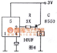
ND-1 amplification circuit diagram
Published:2014/4/16 20:39:00 Author:lynne | Keyword: ND-1 amplification circuit diagram
Amplified by the transistor drive current relay or power load.
(View)
View full Circuit Diagram | Comments | Reading(1207)
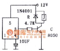
ND-1 produced by human motion detector circuit diagram
Published:2014/4/15 22:50:00 Author:lynne | Keyword: ND-1 produced by human motion detector circuit diagram
ND-1 produced by human motion detector, Figure, when the body is in constant motion when, ND-1 output is high, and through the internal circuit delay, when the body stops moving, ND-1 output into low, C8550 conduction, alarm circuit B to work, sound an alarm, this circuit can be developed into old ambulance alarm, military field ambulance, such as the alarm circuit switch wireless transmitter that can be used stolen object tracker or tracking animals were observed instruments and other electronic alarm and detection devices.
(View)
View full Circuit Diagram | Comments | Reading(1313)
ND-1 with output pulse signal application circuit
Published:2014/4/15 22:49:00 Author:lynne | Keyword: ND-1 with output pulse signal application circuit
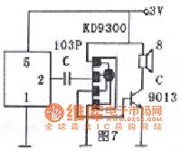
With the application of ND-1 output pulse signal, shown in Figure, which can be set up in a musical doorbell on the door (or alarm) circuit, when guests knock on the door, ND-1 can trigger pulse output string music ICKD9300 work play a role doorbell, if someone in the door lock picking or unauthorized intrusion, the circuit will be action, play a security role, the power consumption of the entire circuit is UA level, with an oscilloscope to see P2 pin output waveform.
(View)
View full Circuit Diagram | Comments | Reading(1195)
Timer switch circuit diagram
Published:2014/4/15 22:48:00 Author:lynne | Keyword: Timer switch circuit diagram, XR2242
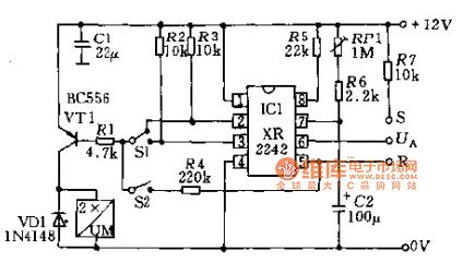
Monolithic circuit shown in FIG time transmitter circuit XR2242, timing time from a few milliseconds to a few days. The circuit comprises a time base oscillator, a binary counter 8 and a control trigger. Time base circuit by the resistor R and the capacitor C form, can have T = RC (pin 8). T = 2RC (pin 2) and T = 128RC (pin 3) three output pulse time by the applied voltage, the output can be reset automatically, use the flip-flop positive edge of the input pulse time can start the process. circuit output terminal (pin 6) voltage UA is low, so that the external action relays and other components. 6 may also be connected to the foot end of the R or S, the electric set or reset (switch S2 together). using the switch S1 can select the delay time. Timer switch circuit diagram shown in Figure:
(View)
View full Circuit Diagram | Comments | Reading(2077)
IR receiver schematic circuit
Published:2014/4/15 22:46:00 Author:lynne | Keyword: IR receiver schematic circuit
IR receiver schematic circuitas shown:
(View)
View full Circuit Diagram | Comments | Reading(3910)
ND specific sensor actual application circuit
Published:2014/4/15 22:41:00 Author:lynne | Keyword: ND specific sensor actual application circuit
This is a solid state sensor is not sound control member, and when subjected to vibration or shaking greatly, its internal resistance will change quickly when added to the bias resistor R, a magnitude of the output voltage to the trigger signal, the signal Music can drive IC, control circuit, volume: 0.8 × 2 × 2.2cm, the application shown in Figure.
(View)
View full Circuit Diagram | Comments | Reading(2866)
| Pages:7/2234 1234567891011121314151617181920Under 20 |
Circuit Categories
power supply circuit
Amplifier Circuit
Basic Circuit
LED and Light Circuit
Sensor Circuit
Signal Processing
Electrical Equipment Circuit
Control Circuit
Remote Control Circuit
A/D-D/A Converter Circuit
Audio Circuit
Measuring and Test Circuit
Communication Circuit
Computer-Related Circuit
555 Circuit
Automotive Circuit
Repairing Circuit