
Circuit Diagram
Index 1506
Three Colors Coding Integrated Circuit of CXA1645M VCD
Published:2011/7/19 10:13:00 Author:Michel | Keyword: Three Colors, Coding Integrated Circuit

CXA1645M is three colors coding integrated circuit of VCD prodcued by SONY,which is widely used in SONY, Samsung and Sharp VCD.
First,Inner Circuit Block Diagram
CXA1645M internal includes color TV signal P/N coding system function and it can output video P/N system full TV signalor blue separation S terminal output signal as long as R, G, B three colors signal and composite synchronous pulse signal are input.The two kinds of output in IC internal have buffer amplifier and the best load is 75 Ω. CXA1645M internal does not set color coding of special color subcarrier oscillator.The special negative carrier generating circuit is used when it is used in the VCD. (View)
View full Circuit Diagram | Comments | Reading(1620)
Function generator circuit
Published:2011/7/17 1:27:00 Author:Fiona | Keyword: Function generator
View full Circuit Diagram | Comments | Reading(499)
Vienna bridge sinusoidal oscillator circuit
Published:2011/7/17 1:26:00 Author:Fiona | Keyword: sinusoidal oscillator

View full Circuit Diagram | Comments | Reading(938)
Free operation trigger circuit
Published:2011/7/17 1:25:00 Author:Fiona | Keyword: trigger, Free operation
View full Circuit Diagram | Comments | Reading(603)
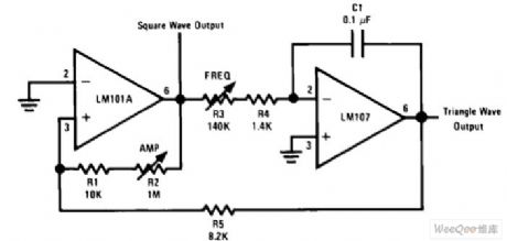
High frequency sine wave generator and orthogonal output circuit
Published:2011/7/17 1:23:00 Author:Fiona | Keyword: High frequency, sine wave generator, orthogonal output

View full Circuit Diagram | Comments | Reading(3543)
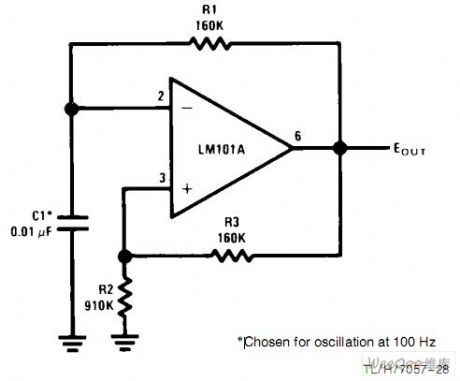
Low frequency sine wave generator and orthogonal output circuit
Published:2011/7/17 1:22:00 Author:Fiona | Keyword: Low frequency, sine wave generator, orthogonal output
View full Circuit Diagram | Comments | Reading(3386)
Safe and reliable multi-function charger circuit
Published:2011/7/18 20:09:00 Author:TaoXi | Keyword: Safe, reliable, multi-function, charger


The principle diagram of this charger is as shown in figure 5-16. The 220V city electricity is reduced by the transformer T, and it is bridge rectified by the diodes VD1-VD4 to output the 17V, 100Hz pulsating DC voltage, this DC voltage can supply the power to the charging circuit. The DC current is stabilized by IC1 to supply power to the time-base integrated circuit IC2(NE555), so the IC2(NE555) produces the oscillation, we can use the pulse signal which is output by the pin-3 to control the conduction and cut-off of the darlington tube which is composed of the VT1 and VT2. This circuit has the RP, the electric potential of the adjustable port of it can be used to set the recharging the battery benchmark voltage.
(View)
View full Circuit Diagram | Comments | Reading(598)
Safe automatic nickel cadmium battery charger circuit
Published:2011/7/18 19:56:00 Author:TaoXi | Keyword: Safe, automatic, nickel cadmium battery, charger

The circuit is as shown in figure 4-21. The IC2(CD4060) is the 14-bit binary serial counter/frequency divider, the IC2(CD4060) and the VT1, K control the charging time. The C4, R4 are the reset circuit of IC2. IC3 is the 555 manifold block, it forms the oscillator which has small duty ratio, and the pulse constant current charging and discharging circuit is composed of the IC3, VT2, VT3 and VT4. By using this kind of circuit, we can charge the battery with large current to shorten the charging time and eliminate the memory effect of the battery. By changing the R10 and R11, we can change the charging and discharging current. LED2 controls the VT2 and VT3 to do the constant current charging.
(View)
View full Circuit Diagram | Comments | Reading(981)
Commonly used slow charger circuit principle diagram
Published:2011/7/18 19:41:00 Author:TaoXi | Keyword: Commonly used, slow charger, circuit, principle diagram

The 220V voltage is limited by the capacitor C1 and rectified by the diode to become the pulsating current, this pulsating current achieves the purpose of battery charging and charging indication through the batteries and ED network. Because the capacitor capacitive reactance is larger than the charging loop impedance, the loop current is decided by the value of C1, so this charging mode is the constant-current type, the value of capacitor C1 is 0.47uF, the charging current is about 30mA. The ED network is the charging indication circuit, R2 has the shunting effect. The electrolytic capacitor C2 has the energy storage effect. The resistor R1 is the bleeder resistance of C1.
(View)
View full Circuit Diagram | Comments | Reading(571)
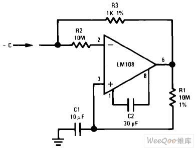
Rapid integration low input current circuit
Published:2011/7/17 22:58:00 Author:Fiona | Keyword: low input current
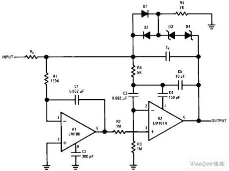
Rapid integration low input current circuit is shown as above:
(View)
View full Circuit Diagram | Comments | Reading(420)
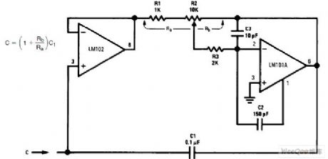
Q adjustable notching filter circuit
Published:2011/7/17 2:03:00 Author:Fiona | Keyword: notching filter

Q adjustable notching filter circuit is shown as above:
(View)
View full Circuit Diagram | Comments | Reading(748)
High power adjustable charger circuit
Published:2011/7/18 19:27:00 Author:TaoXi | Keyword: High power, adjustable, charger, circuit

The principle of this charging device is as shown in figure 3-7, the maximum output current is 20A, the highest charging voltage is 80V. It can be adjusted from 0V, so it can charge all kinds of batteries and the battery groups or battery groups in series which have the same specifications, such as five 12V batteries in series. By charging the series batteries, we can shorten the length of wiring and reduce the power consumption, so the operating efficiency is improved.
(View)
View full Circuit Diagram | Comments | Reading(621)
Two-stage tuning circuit
Published:2011/7/17 22:56:00 Author:Fiona | Keyword: Two-stage, tuning
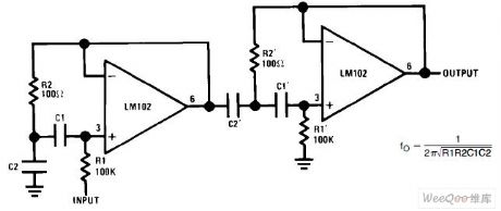
Two-stage tuning circuit is shown as above:
(View)
View full Circuit Diagram | Comments | Reading(636)
Automatic battery charger circuit with the voltage instruction
Published:2011/7/18 5:03:00 Author:TaoXi | Keyword: Automatic, battery charger, voltage instruction

The circuit is as shown in figure 4-6. IC is the LED electrical level indication integrated circuit which has ten output instruction ports. When the signal is added on the pin-5 of the output port, the internal circuit of this IC will compare the signal voltage and report the result through the level situation of the output port. If you connect the LEDs with every port of the IC, the LED can intuitively report the input signal voltage. The transistors VT1-VT5 can be used to detect the levels of the IC's output ports. When the output port which is connected with the transistor base has the low level, this transistor will conduct, the power will charge the battery through the c, e junctions and the current limiting resistance.
(View)
View full Circuit Diagram | Comments | Reading(622)
Negative capacitance multiplier circuit
Published:2011/7/17 22:55:00 Author:Fiona | Keyword: Negative capacitance, multiplier
Negative capacitance multiplier circuit is shown as above:
(View)
View full Circuit Diagram | Comments | Reading(2126)
Automatic charger circuit with the manual trigger function
Published:2011/7/18 3:42:00 Author:TaoXi | Keyword: Automatic, charger, manual, trigger function

Operating principle:
The circuit is as shown in figure 4-5. The city electricity is reduced by transformer T, the subprime output voltage is rectified by the bridge type rectifier circuit which is composed of the VD1-VD4, and then it is filted by the C1 to be the DC voltage, at last it produce the +5V stable voltage through IC1: it can be used as the reference voltage of the control circuit, and it also supplies the operating power to IC2. At the same time, the bridge rectifier is divided into two parts, and it outputs two groups of inverted half-wave rectified pulsating voltage through the two ends of the secondary coil to charge the four Nickel-cadmium batteries respectively. The LED1 can be used as the charging indicator light, the R6, R7, R8 are the current-limiting resistance.
(View)
View full Circuit Diagram | Comments | Reading(660)
Varactor multiplier circuit
Published:2011/7/17 22:53:00 Author:Fiona | Keyword: Varactor multiplier
Varactor multiplier circuit is shown as above:
(View)
View full Circuit Diagram | Comments | Reading(496)
Photodiode amplifier circuit
Published:2011/7/17 2:01:00 Author:Fiona | Keyword: Photodiode, amplifier

Photodiode amplifier circuit is shown as above:
(View)
View full Circuit Diagram | Comments | Reading(2390)
Single-tube constant current charger circuit
Published:2011/7/18 3:27:00 Author:TaoXi | Keyword: Single-tube, constant current, charger

The practical single-tube constant current charger is as shown in figure 2-20, the transistor VT1 has the function of constant current, the constant current value is decided by the voltage of the regulator tube and R2, the voltage regulator tube uses the 3.3V regulator tube, the resistance R2 is (30Ω-60Ω)/(1W-2W), at this time the charging current is about 50mA-80mA. The charging indicator circuit is composed of the R3(200Ω-500Ω) and LED, as long as you connect the rechargeable batteries to the circuit, the LED will turns on. If the LEd will not turn on, the battery is bad. This circuit can charge one to four Number five nickel cadmium batteries, the charging time is 12-14 hours. The transistor VT1 can use the 3DD15 or DS11 power tube.
(View)
View full Circuit Diagram | Comments | Reading(894)
Low cost and high reliability electric bicycle charger circuit
Published:2011/7/18 3:12:00 Author:TaoXi | Keyword: Low cost, high reliability, electric bicycle, charger


The MC3842 is designed as one kind of 8-pin single port output other-excited switch power driving integrated circuit, the internal circuit is composed of the benchmark voltage regulator, the error amplifier, the pulse width comparator, the latch, the oscillator, the pulse width modulator, the pulse output driver stage.etc. The MC3842 some similar products, the interchangeable products are UC3842, IR3842N, SG3842, CM3842, LM3842.etc. The
The internal block diagram of MC3842 is as shown in figure 1.
The single-ended PWM pulse output, the output driving current is 200mA, the peak current can be 1A.
The start voltage is more than 16V, the 1mA start current can make the circuit get into the operating state.
It has the 5V/50mA reference voltage source.
(View)
View full Circuit Diagram | Comments | Reading(2270)
| Pages:1506/2234 At 2015011502150315041505150615071508150915101511151215131514151515161517151815191520Under 20 |
Circuit Categories
power supply circuit
Amplifier Circuit
Basic Circuit
LED and Light Circuit
Sensor Circuit
Signal Processing
Electrical Equipment Circuit
Control Circuit
Remote Control Circuit
A/D-D/A Converter Circuit
Audio Circuit
Measuring and Test Circuit
Communication Circuit
Computer-Related Circuit
555 Circuit
Automotive Circuit
Repairing Circuit