
Switch Control
Index 2
High Current Switching Regulator Made Of DN-41
Published:2011/9/6 6:52:00 Author:Felicity | Keyword: High Current, Switching Regulator

View full Circuit Diagram | Comments | Reading(671)
Ultrasonic remote light switch circuit diagram
Published:2011/8/9 18:03:00 Author:Vicky | Keyword: ultrasonic, remote light switch
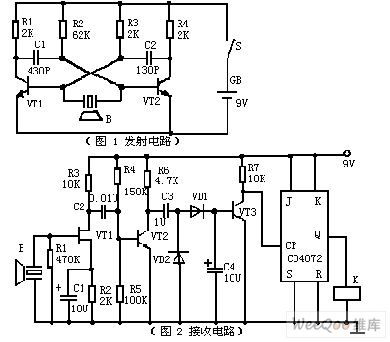
Picture 1 is a emitter circuit. The circuit uses discrete devices. VT1, VT1, R1, R2, R3, R4 , C1 and C2 constitute a self-excitation multivibrator. Ultrasonic emitting device B is connected in the collector loop of VT1 and VT2 to conduct push-pull work. The time of loop is often determined by R1, C1, R4 and C2. The resonance frequency of ultrasonic receptor device B triggers the multivibrator circuit. Hence, the circuit can work under optimized frequency.
Picture 2 is a receiving circuit, JFET VT1 constitutes high-input resistance amplifier, which performs better working with ultrasonic receptor device B and obtains higher receiving sensitiveness and better frequency-selecting performance. (View)
View full Circuit Diagram | Comments | Reading(1514)
Touch relay switch circuit diagram
Published:2011/8/4 21:11:00 Author:Sophia | Keyword: Touch relay switch

Touch delay switch circuit formed by the time base NE555 chip.
IC1 is a 555 timer circuit, which also becomes monostablecircuit. Usually because P-side of touching film doesn't have induced voltage, which make capacitor C1 discharge through the 7th foot of 555 , 3-pin output is low level. The relay KS is released, and light does not shine.
When you need to turn on the lights, we just touch the metal P with the hands. The noise signal voltage of the human sense is added from C2 to the trigger terminal of 555, which makes the output of 555 become high from low output, relay KS pull and light lightened. Meanwhile, the first 7 pin interior of 555 within is stoped, then the power charge to C1 through R1, and this is the beginning of time. (View)
View full Circuit Diagram | Comments | Reading(3703)
TOUCH_TONE_IC
Published:2009/7/14 21:14:00 Author:May

MOSTEK MK5085/6 IC and keyboard together form inexpensive Touch-Tone generator producing tones within 0.75% of required values. Uses 3.579545-MHz TV color-burst crystal. Pin 15 is grounded to provide dual tones only .Pin 10 provides output when keyboard entry has been made ,for keying push-to-talk (PTT) Loudspeaker can be eliminated if output if fed directly into microphone input of transmitter. Choice of IC depends on type of keyboard used.-T. Ahrens, Integrated-Circuit Tone Generator, Ham Radio, Feb. 1977, p70. (View)
View full Circuit Diagram | Comments | Reading(2809)
TOUCH_SWITCH_II
Published:2009/7/14 19:57:00 Author:May

IC1, a 555 timer, is connected in a one-shot multivibrator circuit that is triggered by touching the touch terminal. The timed ON period is about 4 seconds with the component values given. To increase the ON time, increase the value of R3 or C2; to decrease the ON time, reduce the value of R3 or C2. The 9-V output at IC1 pin 3 can be used to drive an optocoupler, a power transistor, a hexFET transistor, CMOS circuitry, and more. (View)
View full Circuit Diagram | Comments | Reading(0)
TUNING_BY_REACTANCE_SWITCHING
Published:2009/7/14 20:31:00 Author:May

Tuning voltage V, in range of 0 to 7 V changes effective capacitance during peak positive portion of collector voltage cycle, to provide tuning over range of about 90 to 150 MHz. Reactance-switching HP 5082-3188 diode CR1 switches in additional capacitance for oscillator using Motorola 2N5208 transistors.-C. Weber, VCO Reactance Switching Provides Broad Tuning Range, EDN Magazine, March 20, 1977, p 151 and 153. (View)
View full Circuit Diagram | Comments | Reading(682)
TOUCH_SWITCH_Ⅲ
Published:2009/7/14 20:14:00 Author:May

The touch switch shown uses 9-Vdc operation, rather than the commonly used 120-Vac. (View)
View full Circuit Diagram | Comments | Reading(712)
SIMPLE_TOUCH_SWITCH
Published:2009/7/14 20:13:00 Author:May

This circuit has two high-gain transistors. Operation occurs when the ambient 60-Hz ac field is impressed on the touch pad during the finger contact. The signal turns on Q1, causing Q2 to energize the relay. Capacitor C1 is used to prevent the relay from oscillating. (View)
View full Circuit Diagram | Comments | Reading(0)
ALTERNATIVE_LIGHT_OPERATED_TURNOFF_TOUCH_SWITCH
Published:2009/7/14 20:11:00 Author:May

When the touch plate is touched, it turns the output of IC1 on, giving a positive potential to the base of Q2. In turn, that turns on pins 4, 5, and 6 of IC2, triggering the SCR's gate and energizing RY1.When RY1 is energized, its contacts pull in, turning on the ac bulb. When R1 is hit by a strong light, it turns on the SCR and energizes RY1. To turn the ac bulb off, just point a strong flashlight at R2; this decreases the base resistance of Q3, making its base positive and, therefore, energizing RY2. When the contact of RY2 pulls in, it disconnects the anode of the SCR from the positive supply, turning it off. Or you can press S2 to energize RY2 and turn off the ac bulb (View)
View full Circuit Diagram | Comments | Reading(1536)
SWITCH_OPERATED_TURNOFF_TOUCH_SWITCH
Published:2009/7/14 20:08:00 Author:May

When S1 is closed,the circuitry is on in standby mode.When the touch plate is touched,the output of the 555 time IC1 goes high,supplying a positive potential to the base of transistor Q2,aiding its bias,The transistor is then on,allowing current to flow through pin4,5 and 6 of IC2.The gate of the SCR is then triggered,the relay is energized,and its contacts turn the ac bulb on.To turn the bulb off,just press S2(RESET),which disconnects the ande of the SCR from the positive supply,turning it off and deenergizing the relay,The light-dependent resistor(R7)is used if you want to turn on the circuit remotely.Just point a flashinght at R7 to decrease its resistance,leaving only the 1000Ω resistor as the base resistance.The resistance give the base a positive positive potential,forward biasing the emitter-base junction of transistor Q1.Transistor Q2 is also turned on because its base is made positive by Q1,which triggers SCR1,energizing the relay.
(View)
View full Circuit Diagram | Comments | Reading(1331)
LIGHT_OPERATED_TURNOFF_TOUCH_SWITCH
Published:2009/7/14 20:00:00 Author:May

When R5 is illuminated by a flashlight, its resistance lowers, leaving only 10,000Ω as the minimum base resistance. That process gives a positive potential to the base of Q1, therefore turning on the transistor, activating RY2, and turning off the SCR. Or you can press S1 to turn the circuitry off. (View)
View full Circuit Diagram | Comments | Reading(759)
TOUCH_SWITCH_I
Published:2009/7/14 19:50:00 Author:May

This touch switch controls an ac-powered bulb, and requires only a few parts. Touching the touch plate triggers the SCR's gate, turning it on and allowing current to flow from the cathode to the anode of SCR1, thereby activating the relay. (View)
View full Circuit Diagram | Comments | Reading(0)
ONE_BUTTON_LATCHING_SWITCH
Published:2009/7/14 12:13:00 Author:May


The SET and RESET inputs are grounded, the inverted (-Q) output is fed back to the D input, and the pulses go into the CLOCK input. Each positive pulse makes the flip-flop toggle from one state to the other. The TLC555 chip in the ftgure serves two purposes. It inverts the pulses so that you can get a positive pulse from a switch that is connected to ground. More importantly, it also debounces the switch. When you press a button, it doesn't just make contact once-the contacts bounce, opening and closing three or four times. The 4013 would toggle once on each bounce, leading to unpredictable results. Thp TLC555 uses a resistor and capacitor to smooth out these fluctuations so that each press of the button produces only one pulse. (View)
View full Circuit Diagram | Comments | Reading(2276)
LATCHING_SWITCH_CIRCUIT
Published:2009/7/14 12:06:00 Author:May

One button turns the LED on, the other turns it off. If you apply a positive pulse to the SET input, the output tums on. It remains on until a positive pulse is applied to the RESET input to turn it off. (TTL flip-flops such as the 74LS74 are actuated by negative, rather than positive pulses.) (View)
View full Circuit Diagram | Comments | Reading(2770)
33_kW_SWITCHING
Published:2009/7/14 4:12:00 Author:May

Delco DTS-518 and DTS-519 power transistors in high-efficiency stacked supply are operated at 25-kHz switching rate to provide 330 VDC at 10 A. Control circuit operates at primary 50-kHz pulse frequency, with negative-going pulses having 2-μs duration. Flip-flop converts this to 25-kHz complementary square-wave signal driving Darlington DTS-2000s. Transformer cores are Magnetics EE No. 42510 each having 15-tum primary and 5-tum secondary for driving DTS-518s. Error amplifier compares portion of total output voltage to zener reference for control of DTS-519 power transistor switching at 25 kHz. Efficiency is 95% at full Ioad.- 3.3kW High Efficiency Switch Mode Regulator, Delco, Kokomo, IN, 1977, Application Note 59. (View)
View full Circuit Diagram | Comments | Reading(842)
BIAS_SWITCH
Published:2009/7/14 4:01:00 Author:May

Automatic electronic bias switching improves efficiency of negatively biased linear class B RF power amplifier such as Heath SB-200 because no power is dissipated under no-signal conditions. Transistors are chosen to withstand maximum negative voltages switched, about -150 VDC. Capacitor across collector-base junction of Q1 can be adjusted to reduce turn-on time of switch. With no RE drive from transmitter, amplifier is biased to cutoff and plate current is zero. Switch will operate at RF threshold of about 2 V and apply class B bias voltage to amplifier. As RF drive is increased, plate current increases. With transmitter in SSB mode, plate current is zero with no speech. For speech, plate current increases with RF driving voltage.-F. E. Hinkle, Electronic Bias Switch for Negatively Biased Amplifiers, Ham Radio, Nov, 1976, p 27-29. (View)
View full Circuit Diagram | Comments | Reading(1590)
150_W_SWITCH_MODE
Published:2009/7/14 3:47:00 Author:May

Unregulated DC voltage is applied to power Darlington Q1 serving as switch that chops voltage so rectangular waveform is applied to RLC output filter. Average voltage to filter depends on duty cycle of switch. 555 timer operates in mono MVBR mode as pulse generator and pulse-duration modulator. R24 applies varying voltage to pin 5 to modulate pulse duration linearly with respect to applied voltage, Actions of O1, Q2, and Q6 maintain constant 3.6 V at arm of control pot. Q4 and Q5 provide 20-kHz clock pulse, above audible range. Overcurrent protection of transistors is provided by R11, SCR, and Q3. Adjust R11 so SCR turns on and shuts down circuit when current through R11 reaches 8 A. Circuit must be reset manually after overload. Q7 and R10 load circuit to prevent oscillation at low output volt-age and light load.-R. J. Walker, A 150 Watt Switch-Mode Regulator, CQ, March 1977, p 40-43 and 74-75. (View)
View full Circuit Diagram | Comments | Reading(947)
5_kW_SWITCHING
Published:2009/7/14 3:49:00 Author:May

Six Delco DTS-709 transistors are connected in progressive Darlington configuration to provide stable and efficient switching at high voltages. Can be operated from 480-V three-phase full-wave rectified line to minimize filter cost. Control circuit uses one LM3900 IC operating from isolated 15-V supply, along with 5-kHz triangle oscillator and error sensor feeding into comparator. In power stage, one DTS-709 drives two DTS-709s which drive three DTS-709s. Efficiency is better than 90% for all loads above 500 W.- Economical 5 kW Switching Regulator Using DT'S-709 Transistors, Delco, Kokomo, IN, 1974, Application Note 56. (View)
View full Circuit Diagram | Comments | Reading(686)
REFERENCE_SWITCH
Published:2009/7/14 3:32:00 Author:May


Provides low-zero-offset 5-microsec pulses with stabilized amplitude, obtained from synchronous flip-flop. Output pulses switch from zero to -5 v, for driving compute and hold amplifiers of serial decoder,-R. M.Centner and J. R. Wilkinson, New Approach to Serial Decoding Eliminates Static Storage, Electronics, 35:34, p 32-35. (View)
View full Circuit Diagram | Comments | Reading(741)
REDUCING_24_V_TO_5_V
Published:2009/7/14 3:29:00 Author:May

Uses Fairchild μA78S40 switching regulator having variety of internal functions that can provide differing voltage step-up, step-down, and inverter modes by appropriately connecting external components. Connections shown provide step-down from 24 V to 5 V at 500 mA with 83% efficiency. Applications include running TTL from 24-V battery. Output ripple is less than 25 V. Article gives design equations.-R. J. Apfel and D. B. Jones, Universal Switching Regulator Di-versifies Power Subsystem Applications, Computer Design, March 1978, p 103-112. (View)
View full Circuit Diagram | Comments | Reading(675)
| Pages:2/15 123456789101112131415 |
Circuit Categories
power supply circuit
Amplifier Circuit
Basic Circuit
LED and Light Circuit
Sensor Circuit
Signal Processing
Electrical Equipment Circuit
Control Circuit
Remote Control Circuit
A/D-D/A Converter Circuit
Audio Circuit
Measuring and Test Circuit
Communication Circuit
Computer-Related Circuit
555 Circuit
Automotive Circuit
Repairing Circuit