Want to post a buying lead? If you are not a member yet, please select the specific/related part number first and then fill the quantity and your contact details in the "Request for Quotation Form" on the left, and then click "Send RFQ".Your buying lead can then be posted, and the reliable suppliers will quote via our online message system or other channels soon.
Offered in 512Mx8bit, the K9F4G08U0M is a 4G-bit NAND Flash Memory with spare 128M-bit. Its NAND cell provides the most costeffective solution for the solid state application market. A program operation can be performed in typical 200s on the (2K+64)Byte page and an erase operation can be performed in typical 1.5ms on a (128K+4K)Byte block. Data in the data page can be read out at 25ns cycle time per Byte. The I/O pins serve as the ports for address and data input/output as well as command input. The on-chip write controller automates all program and erase functions including pulse repetition, where required, and internal verification and margining of data. Even the write-intensive systems can take advantage of the K9F4G08U0Ms extended reliability of 100K program/ erase cycles by providing ECC(Error Correcting Code) with real time mapping-out algorithm. The K9F4G08U0M is an optimum solution for large nonvolatile storage applications such as solid state file storage and other portable applications requiring non-volatility.
K9F4G08U0M Maximum Ratings
Parameter
Symbol
Rating
Unit
-0.6 to + 4.6
Voltage on any pin relative to VSS
VIN/OUT
V
VCC/VCCQ
-0.6 to + 4.6
Temperature Under Bias
K9F4G08U0M-XCB0
TBIAS
-10 to +125
K9F4G08U0M-XIB0
-40 to +125
Storage Temperature
K9F4G08U0M-XCB0
TSTG
-65 to +150
K9F4G08U0M-XIB0
Short Circuit Current
IOS
5
mA
NOTE : 1. Minimum DC voltage is -0.6V on input/output pins. During transitions, this level may undershoot to -2.0V for periods <30ns. Maximum DC voltage on input/output pins is VCC+0.3V which, during transitions, may overshoot to VCC+2.0V for periods <20ns. 2. Permanent device damage may occur if ABSOLUTE MAXIMUM RATINGS are exceeded. Functional operation should be restricted to the conditions as detailed in the operational sections of this data sheet. Exposure to absolute maximum rating conditions for extended periods may affect reliability.
K9F4G08U0M Features
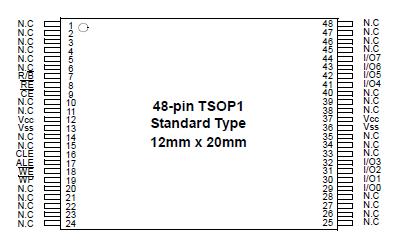
• Voltage Supply - 2.70V ~ 3.60V • Organization - Memory Cell Array : (512M + 16,384K)bit x 8bit - Data Register : (2K + 64)bit x 8bit • Automatic Program and Erase - Page Program : (2K + 64)Byte - Block Erase : (128K + 4K)Byte • Page Read Operation - Page Size : (2K + 64)Byte - Random Read : 20s(Max.) - Serial Access : 25ns(Min.) 512M x 8 Bit / 1G x 8 Bits NAND Flash Memory • Fast Write Cycle Time - Page Program time : 200s(Typ.) - Block Erase Time : 1.5ms(Typ.) • Command/Address/Data Multiplexed I/O Port • Hardware Data Protection - Program/Erase Lockout During Power Transitions • Reliable CMOS Floating-Gate Technology - Endurance : 100K Program/Erase Cycles - Data Retention : 10 Years • Command Driven Operation • Intelligent Copy-Back with internal 1bit/528Byte EDC • Unique ID for Copyright Protection • Package : - K9F4G08U0M-YCB0/YIB0 48 - Pin TSOP I (12 x 20 / 0.5 mm pitch) - K9F4G08U0M-PCB0/PIB0 : Pb-FREE PACKAGE 48 - Pin TSOP I (12 x 20 / 0.5 mm pitch) - K9F4G08U0M-ICB0/IIB0 52 - Pin ULGA (12 x 17 / 1.00 mm pitch) - K9K8G08U1M-ICB0/IIB0 52 - Pin ULGA (12 x 17 / 1.00 mm pitch)