Want to post a buying lead? If you are not a member yet, please select the specific/related part number first and then fill the quantity and your contact details in the "Request for Quotation Form" on the left, and then click "Send RFQ".Your buying lead can then be posted, and the reliable suppliers will quote via our online message system or other channels soon.
Drain to Source Voltage (Note 1) .......................... VDSS 100 V Drain to Gate Voltage (RGS = 20k) (Note 1).................... VDGR 100 V Gate to Source Voltage ............................... VGS ±20 V Drain Current Continuous (TA = 25, VGS = 10V)(Figure 2) ......................ID44 A Continuous (TA = 100, VGS = 10V) (Figure 2) ......................ID31A Pulsed Drain Current ................................IDM Figure 4 Pulsed Avalanche Rating ...........................ULS Figure6,14,15 Power Dissipation ...................................PD155W Derate Above 25 ..................................1.03 W/ Operating and Storage Temperature ...................TJ, TSTG -55 to 175 Maximum Temperature for Soldering Leads at 0.063in (1.6mm) from Case for 10s .....................TL 300 Package Body for 10s, See Techbrief 334 ........ ..............Tpkg 260 NOTE: 1. TJ = 25 to 150 CAUTION: Stresses above those listed in "Absolute Maximum Ratings" may cause permanent damage to the device. This is a stress only rating and operation of the device at these or any other conditions above those indicated in the operational sections of this specification is not implied. .
HUFA75637P3 Features
• Ultra Low On-Resistance - rDS(ON) = 0.030, VGS = 10V • Simulation Models - Temperature Compensated PSPICE® and SABER™Electrical Models - Spice and SABER Thermal Impedance Models - www.fairchildsemi.com • Peak Current vs Pulse Width Curve • UIS Rating Curve
HUFA75637S3S Parameters
Technical/Catalog Information
HUFA75637S3S
Vendor
Fairchild Semiconductor
Category
Discrete Semiconductor Products
Mounting Type
Surface Mount
FET Polarity
N-Channel
Drain to Source Voltage (Vdss)
100V
Current - Continuous Drain (Id) @ 25° C
44A
Rds On (Max) @ Id, Vgs
30 mOhm @ 44A, 10V
Input Capacitance (Ciss) @ Vds
1700pF @ 25V
Power - Max
155W
Packaging
Tube
Gate Charge (Qg) @ Vgs
108nC @ 20V
Package / Case
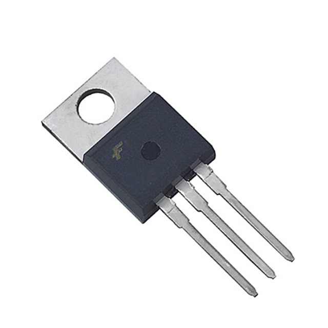
D²Pak, SMD-220, TO-263 (2 leads + tab)
FET Feature
Standard
Lead Free Status
Lead Free
RoHS Status
RoHS Compliant
Other Names
HUFA75637S3S HUFA75637S3S
HUFA75637S3S Maximum Ratings
Drain to Source Voltage (Note 1) .......................... VDSS 100 V Drain to Gate Voltage (RGS = 20k) (Note 1).................... VDGR 100 V Gate to Source Voltage ............................... VGS ±20 V Drain Current Continuous (TA = 25, VGS = 10V)(Figure 2) ......................ID44 A Continuous (TA = 100, VGS = 10V) (Figure 2) ......................ID31A Pulsed Drain Current ................................IDM Figure 4 Pulsed Avalanche Rating ...........................ULS Figure6,14,15 Power Dissipation ...................................PD155W Derate Above 25 ..................................1.03 W/ Operating and Storage Temperature ...................TJ, TSTG -55 to 175 Maximum Temperature for Soldering Leads at 0.063in (1.6mm) from Case for 10s .....................TL 300 Package Body for 10s, See Techbrief 334 ........ ..............Tpkg 260 NOTE: 1. TJ = 25 to 150 CAUTION: Stresses above those listed in "Absolute Maximum Ratings" may cause permanent damage to the device. This is a stress only rating and operation of the device at these or any other conditions above those indicated in the operational sections of this specification is not implied. .
HUFA75637S3S Features
• Ultra Low On-Resistance - rDS(ON) = 0.030, VGS = 10V • Simulation Models - Temperature Compensated PSPICE® and SABER™Electrical Models - Spice and SABER Thermal Impedance Models - www.fairchildsemi.com • Peak Current vs Pulse Width Curve • UIS Rating Curve