HCF4502BF, HCF4503, HCF4503BE Selling Leads, Datasheet
MFG:SGS Package Cooled:DIP D/C:85

HCF4502BF, HCF4503, HCF4503BE Datasheet download

Part Number: HCF4502BF
MFG: SGS
Package Cooled: DIP
D/C: 85


MFG:SGS Package Cooled:DIP D/C:85
HCF4502BF, HCF4503, HCF4503BE Datasheet download
MFG: SGS
Package Cooled: DIP
D/C: 85

Want to post a buying lead? If you are not a member yet, please select the specific/related part number first and then fill the quantity and your contact details in the "Request for Quotation Form" on the left, and then click "Send RFQ".Your buying lead can then be posted, and the reliable suppliers will quote via our online message system or other channels soon.
TOP
PDF/DataSheet Download
Datasheet: HCF4000
File Size: 296944 KB
Manufacturer: STMICROELECTRONICS [STMicroelectronics]
Download : Click here to Download
PDF/DataSheet Download
Datasheet: HCF4503
File Size: 87345 KB
Manufacturer: STMICROELECTRONICS [STMicroelectronics]
Download : Click here to Download
PDF/DataSheet Download
Datasheet: HCF4503BEY
File Size: 87345 KB
Manufacturer: STMICROELECTRONICS [STMicroelectronics]
Download : Click here to Download
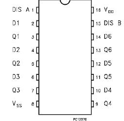
The HCF4503B is a monolithic integrated circuits, available in 16-lead dual in-line plastic package and plastic micro package.
The HCF4503B is a hex noninverting buffer with 3-state outputs having high sink and source-current capability. Two disable controls are provided, one of which controls four buffers and the other controls the remaining two buffers.
|
Symbol |
Parameter |
Value |
Unit |
|
VDD* |
Supply Voltage |
0.5 to + 18 |
V |
|
Vi |
Input Voltage |
0.5 to VDD + 0.5 |
V |
|
II |
DC Input Current (any one input) |
± 10 |
mA |
|
Pt ot |
Total Power Dissipation (per package) Dissipation per Output Transistor for Top = Full Package-temperature Range |
200 100 |
mW mW |
|
Top |
Operating Temperature |
-40 to +85 |
°C |
|
Ts tg |
Storage Temperature |
65 to + 150 |
°C °C |
Stresses above those listedunder "AbsoluteMaximum Ratings" may cause permanent damage to thedevice. This isa stress rating only and functional operation ofthedevice atthese or any other conditions above those indicated in the operational sections of this specification is not implied.Exposure to absolute maximumratingconditions for external periodsmayaffect device reliability.
* Allvoltage values are referred toVSS pin voltage

Price: 4-6 USD
MT58L64L18CT-10 TQFP100

Price: 5-6.5 USD
DL-7140-211M laser tube

Price: 4-5 USD
74LVC74APG - IC FLIP FLOP D-Type POS-EDG DUAL 14TSSOP

Price: 6.5-8 USD
CYPRESS - Clock Synthesizer with Differential CPU Outputs

Price: 0.284-0.286 USD
PI5V330QEX Pericom Multiplexer Switch ICs

Price: 1-2 USD
IGBT power module, Single switch, 1200 V, Collector-emitter voltage, 430A

Price: 1-2 USD
a-Si TFT-LCD, NEC, 228.096Hmm, 560V

Price: 0.124-0.2 USD
PC354N1T - Mini-flat Package, AC Input Type Photocoupler - Sharp Electrionic Components

Price: 0.177-0.178 USD
RL1210JR51-XX-BL - Thick Film Chip Resistor Low Ohmic - TAITRON Components Incorporated

Price: 0.053-0.055 USD
STPS140A - POWER SCHOTTKY RECTIFIER - STMicroelectronics

Price: 1.45-1.5 USD
STA013 - MPEG 2.5 LAYER III AUDIO DECODER - STMicroelectronics

Price: 0.073-0.075 USD
SMBJ5347B - 5 Watt Surface Mount Silicon Zener Diodes - Micro Commercial Components
