Want to post a buying lead? If you are not a member yet, please select the specific/related part number first and then fill the quantity and your contact details in the "Request for Quotation Form" on the left, and then click "Send RFQ".Your buying lead can then be posted, and the reliable suppliers will quote via our online message system or other channels soon.
This N-Channel MOSFET has been designed specifically to improve the overall efficiency of DC/DC converters using either synchronous or conventional switching PWM controllers. It has been optimized for low gate charge, low rDS(ON) and fast switching speed.
Thermal Resistance Junction to Case TO-252 Thermal Resistance Junction to Ambient TO-252 Thermal Resistance Junction to Ambient TO-252, 1in2 copper pad area
2.14 100 52
°C/W °C/W °C/W
FDD8876 Features
• rDS(ON) = 8.2mΩ, VGS = 10V, ID = 35A • rDS(ON) = 10mΩ, VGS = 4.5V, ID = 35A • High performance trench technology for extremely low rDS(ON) • Low gate charge • High power and current handling capability
FDD8876 Typical Application
• DC/DC converters
FDD8878 Parameters
Technical/Catalog Information
FDD8878
Vendor
Fairchild Semiconductor
Category
Discrete Semiconductor Products
Mounting Type
Surface Mount
FET Polarity
N-Channel
Drain to Source Voltage (Vdss)
30V
Current - Continuous Drain (Id) @ 25° C
40A
Rds On (Max) @ Id, Vgs
15 mOhm @ 35A, 10V
Input Capacitance (Ciss) @ Vds
880pF @ 15V
Power - Max
40W
Packaging
Tape & Reel (TR)
Gate Charge (Qg) @ Vgs
26nC @ 10V
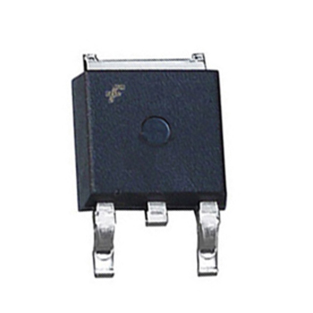
Package / Case
DPak, SC-63, TO-252 (2 leads+tab)
FET Feature
Logic Level Gate
Lead Free Status
Lead Free
RoHS Status
RoHS Compliant
Other Names
FDD8878 FDD8878
FDD8878 General Description
This N-Channel MOSFET has been designed specifically to improve the overall efficiency of DC/DC converters using either synchronous or conventional switching PWM controllers. It has been optimized for low gate charge, low rDS(ON) and fast switching speed.
Thermal Resistance Junction to Case TO-252 Thermal Resistance Junction to Ambient TO-252 Thermal Resistance Junction to Ambient TO-252, 1in2 copper pad area
3.75 100 52
°C/W °C/W °C/W
FDD8878 Features
·rDS(ON) = 15mΩ, VGS = 10V, ID = 35A ·rDS(ON) = 18.5mΩ, VGS = 4.5V, ID = 35A ·High performance trench technology for extremely low rDS(ON) ·Low gate charge ·High power and current handling capability
FDD8878 Typical Application
· DC/DC converters
FDD8880 Parameters
Technical/Catalog Information
FDD8880
Vendor
Fairchild Semiconductor
Category
Discrete Semiconductor Products
Mounting Type
Surface Mount
FET Polarity
N-Channel
Drain to Source Voltage (Vdss)
30V
Current - Continuous Drain (Id) @ 25° C
58A
Rds On (Max) @ Id, Vgs
9 mOhm @ 35A, 10V
Input Capacitance (Ciss) @ Vds
1260pF @ 15V
Power - Max
55W
Packaging
Tape & Reel (TR)
Gate Charge (Qg) @ Vgs
31nC @ 10V
Package / Case
DPak, SC-63, TO-252 (2 leads+tab)
FET Feature
Logic Level Gate
Lead Free Status
Lead Free
RoHS Status
RoHS Compliant
Other Names
FDD8880 FDD8880
FDD8880 General Description
This N-Channel MOSFET has been designed specifically to improve the overall efficiency of DC/DC converters using either synchronous or conventional switching PWM controllers. It has been optimized for low gate charge, low rDS(ON) and fast switching speed.
Thermal Resistance Junction to Case TO-252 Thermal Resistance Junction to Ambient TO-252 Thermal Resistance Junction to Ambient TO-252, 1in2 copper pad area
2.73 100 52
°C/W °C/W °C/W
FDD8880 Features
• rDS(ON) = 9mW, VGS = 10V, ID = 35A • rDS(ON) = 12mW, VGS = 4.5V, ID = 35A • High performance trench technology for extremely low rDS(ON) • Low gate charge • High power and current handling capability