

FDD8796, FDD8870, FDD8874 Selling Leads, Datasheet
MFG:Fairchild Semiconductor Category:Discrete Semiconductor Products Package Cooled:252 D/C:04+
FDD8796, FDD8870, FDD8874 Datasheet download

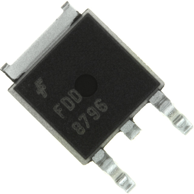
Part Number: FDD8796
Category: Discrete Semiconductor Products
MFG: Fairchild Semiconductor
Package Cooled: 252
D/C: 04+
Description: MOSFET N-CH 30V 116A D-PAK
Price Break
1
10
100
250
500
1000
Unit Price
.92000
.69000
.51750
.38180
.32200
.30590
Extended Price
0.92
6.90
51.75
95.45
161.00
305.90
(All prices are in USD) Prices for reference only


