Want to post a buying lead? If you are not a member yet, please select the specific/related part number first and then fill the quantity and your contact details in the "Request for Quotation Form" on the left, and then click "Send RFQ".Your buying lead can then be posted, and the reliable suppliers will quote via our online message system or other channels soon.
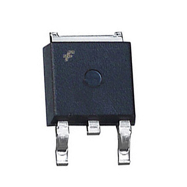
This P-Channel Logic level MOSFET is produced using Fairchild Semiconductor's advanced process that has been especially tailored to minimize the on state resistance and yet maintain low gate charge for superior switching performance.
FDD5202P Maximum Ratings
Symbol
Parameter
Ratings
Units
VDSS VGSS
Drain-Source Voltage Gate-Source Voltage
-60 ±20 -8 -2.3 -15 39 2.8 1.3 -55 to +150
V V A
W
°C
ID
Maximum Drain Current -Continuous TA = 25
(Note 1) (Note 1a)
PD
Maximum Power Dissipation TC = 25 TA = 25 TA = 25
(Note 1) (Note 1a) (Note 1b)
TJ,TSTG
Operating and Storage Junction Temperature Range
FDD5202P Features
• -8 A, -60 V. RDS(on) = 0.3 W @ VGS = -10 V RDS(on) = 0.5 W @ VGS = -4.5 V. • Low gate charge (15.5nC typical). • Fast switching speed.