CX74002-13P, CX74016, CX74017-07P Selling Leads, Datasheet
MFG:CONEXANT Package Cooled:BGA D/C:02+

CX74002-13P, CX74016, CX74017-07P Datasheet download

Part Number: CX74002-13P
MFG: CONEXANT
Package Cooled: BGA
D/C: 02+


MFG:CONEXANT Package Cooled:BGA D/C:02+

CX74002-13P, CX74016, CX74017-07P Datasheet download

MFG: CONEXANT
Package Cooled: BGA
D/C: 02+
Want to post a buying lead? If you are not a member yet, please select the specific/related part number first and then fill the quantity and your contact details in the "Request for Quotation Form" on the left, and then click "Send RFQ".Your buying lead can then be posted, and the reliable suppliers will quote via our online message system or other channels soon.
TOP
PDF/DataSheet Download
Datasheet: CX72300
File Size: 172139 KB
Manufacturer:
Download : Click here to Download
PDF/DataSheet Download
Datasheet: CX74016
File Size: 444225 KB
Manufacturer: Conexant
Download : Click here to Download
PDF/DataSheet Download
Datasheet: CX72300
File Size: 172139 KB
Manufacturer:
Download : Click here to Download
The CX74016 RF/IF Transceiver is a highly integrated, monolithic device optimized for use in Global System for Mobile Communications (GSM) and other Time Division Multiple Access (TDMA) single-band or multi-band applications.
The receive path of the device consists of three Intermediate Frequency (IF) amplifiers with selectable gain, an I/Q demodulator, baseband filters, DC offset compensation circuitry, and selectable gain baseband amplifiers.
The transmit path of the device consists of an In-Phase and Quadrature-Phase (I/Q) modulator and a frequency translation loop designed to perform frequency upconversion with high output spectral purity. The translation loop consists of a phase/frequency detector, a charge-pump, a mixer, and buffers for the required isolation between the RF section, Local Oscillator (LO), and IF inputs.
In addition, the CX74016 features an on-chip dual-loop UHF/VHF frequency synthesizer circuit. It includes two sets of reference dividers, phase/frequency detectors, charge pumps, prescalers, main dividers, lock detector, and control circuits.
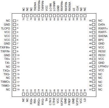
The device package and pin configuration are shown in Figure 1. A block diagram of the CX74016 is shown in Figure 2. The signal pin assignments and functional pin descriptions are found in Table 1.
|
Parameter |
Minimum |
Maximum |
Unit |
| Ambient Operating Temperature |
-30 |
+85 |
°C |
| Storage Temperature |
-50 |
+125 |
°C |
| Power Dissipation |
|
600 |
mW |
| Supply Voltage (VCC) |
0 |
4.5 |
V |
| Input Voltage Range |
GND |
VCC |
V |

