Features: • Quadrature demodulator for downconversion• 80 dB IF gain range and 30 dB baseband gain range• Integrated receive baseband filters with tunable bandwidth• Integrated transmit path with high phase accuracy• Reduced filtering requirements for the transmit pat...
CX74016: Features: • Quadrature demodulator for downconversion• 80 dB IF gain range and 30 dB baseband gain range• Integrated receive baseband filters with tunable bandwidth• Integrat...
SeekIC Buyer Protection PLUS - newly updated for 2013!
268 Transactions
All payment methods are secure and covered by SeekIC Buyer Protection PLUS.
Parameter |
Minimum |
Maximum |
Unit |
Ambient Operating Temperature |
-30 |
+85 |
°C |
Storage Temperature |
-50 |
+125 |
°C |
Power Dissipation |
|
600 |
mW |
Supply Voltage (VCC) |
0 |
4.5 |
V |
Input Voltage Range |
GND |
VCC |
V |
The CX74016 RF/IF Transceiver is a highly integrated, monolithic device optimized for use in Global System for Mobile Communications (GSM) and other Time Division Multiple Access (TDMA) single-band or multi-band applications.
The receive path of CX74016 consists of three Intermediate Frequency (IF) amplifiers with selectable gain, an I/Q demodulator, baseband filters, DC offset compensation circuitry, and selectable gain baseband amplifiers.
The transmit path of CX74016 consists of an In-Phase and Quadrature-Phase (I/Q) modulator and a frequency translation loop designed to perform frequency upconversion with high output spectral purity. The translation loop consists of a phase/frequency detector, a charge-pump, a mixer, and buffers for the required isolation between the RF section, Local Oscillator (LO), and IF inputs.
In addition, the CX74016 features an on-chip dual-loop UHF/VHF frequency synthesizer circuit. It includes two sets of reference dividers, phase/frequency detectors, charge pumps, prescalers, main dividers, lock detector, and control circuits.
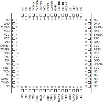
CX74016 package and pin configuration are shown in Figure 1. A block diagram of the CX74016 is shown in Figure 2. The signal pin assignments and functional pin descriptions are found in Table 1.