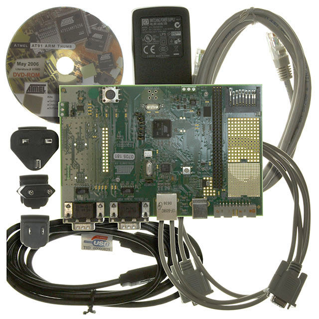
AT91SAM9260 General Description
AT91SAM9260 Features
• Incorporates the ARM926EJ-S™ ARM® Thumb® Processor
DSP Instruction Extensions, ARM Jazelle® Technology for Java® Acceleration
8-KByte Data Cache, 8-KByte Instruction Cache, Write Buffer
200 MIPS at 180 MHz
Memory Management Unit
EmbeddedICE™, Debug Communication Channel Support
• Additional Embedded Memories
One 32-KByte Internal ROM, Single-cycle Access At Maximum Matrix Speed
Two 4-KByte Internal SRAM, Single-cycle Access At Maximum Matrix Speed
• External Bus Interface (EBI)
Supports SDRAM, Static Memory, ECC-enabled NAND Flash and CompactFlash®
• USB 2.0 Full Speed (12 Mbits per second) Device Port
On-chip Transceiver, 2,432-byte Configurable Integrated DPRAM
• USB 2.0 Full Speed (12 Mbits per second) Host Single Port in the 208-lead PQFP Package and Double Port in 217-ball LFBGA Package
Single or Dual On-chip Transceivers
Integrated FIFOs and Dedicated DMA Channels
• Ethernet MAC 10/100 Base T
Media Independent Interface or Reduced Media Independent Interface
28-byte FIFOs and Dedicated DMA Channels for Receive and Transmit
• Image Sensor Interface
ITU-R BT. 601/656 External Interface, Programmable Frame Capture Rate
12-bit Data Interface for Support of High Sensibility Sensors
SAV and EAV Synchronization, Preview Path with Scaler, YCbCr Format
• Bus Matrix
Six 32-bit-layer Matrix
Boot Mode Select Option, Remap Command
• Fully-featured System Controller, including
Reset Controller, Shutdown Controller
Four 32-bit Battery Backup Registers for a Total of 16 Bytes
Clock Generator and Power Management Controller
Advanced Interrupt Controller and Debug Unit
Periodic Interval Timer, Watchdog Timer and Real-time Timer
• Reset Controller (RSTC)
Based on a Power-on Reset Cell, Reset Source Identification and Reset Output Control
• Clock Generator (CKGR)
Selectable 32,768 Hz Low-power Oscillator or Internal Low Power RC Oscillator on Battery Backup Power Supply, Providing a Permanent Slow Clock
3 to 20 MHz On-chip Oscillator, One up to 240 MHz PLL and One up to 130 MHz PLL
• Power Management Controller (PMC)
Very Slow Clock Operating Mode, Software Programmable Power Optimization Capabilities
Two Programmable External Clock Signals
• Advanced Interrupt Controller (AIC)
Individually Maskable, Eight-level Priority, Vectored Interrupt Sources
Three External Interrupt Sources and One Fast Interrupt Source, Spurious Interrupt Protected
• Debug Unit (DBGU)
2-wire UART and Support for Debug Communication Channel, Programmable ICE Access Prevention
• Periodic Interval Timer (PIT)
20-bit Interval Timer plus 12-bit Interval Counter
• Watchdog Timer (WDT)
Key-protected, Programmable Only Once, Windowed 16-bit Counter Running at Slow Clock
• Real-time Timer (RTT)
32-bit Free-running Backup Counter Running at Slow Clock with 16-bit Prescaler
• One 4-channel 10-bit Analog-to-Digital Converter
• Three 32-bit Parallel Input/Output Controllers (PIOA, PIOB, PIOC)
96 Programmable I/O Lines Multiplexed with up to Two Peripheral I/Os
Input Change Interrupt Capability on Each I/O Line
Individually Programmable Open-drain, Pull-up Resistor and Synchronous Output
High-current Drive I/O Lines, Up to 16 mA Each
• Peripheral DMA Controller Channels (PDC)
• One Two-slot MultiMedia Card Interface (MCI)
SDCard/SDIO and MultiMediaCard™ Compliant
Automatic Protocol Control and Fast Automatic Data Transfers with PDC
• One Synchronous Serial Controller (SSC)
Independent Clock and Frame Sync Signals for Each Receiver and Transmitter
I²S Analog Interface Support, Time Division Multiplex Support
High-speed Continuous Data Stream Capabilities with 32-bit Data Transfer
• Four Universal Synchronous/Asynchronous Receiver Transmitters (USART)
Individual Baud Rate Generator, IrDA® Infrared Modulation/Demodulation, Manchester Encoding/Decoding
Support for ISO7816 T0/T1 Smart Card, Hardware Handshaking, RS485 Support
Full Modem Signal Control on USART0
• Two 2-wire UARTs
• Two Master/Slave Serial Peripheral Interfaces (SPI)
8- to 16-bit Programmable Data Length, Four External Peripheral Chip Selects
Synchronous Communications
• Two Three-channel 16-bit Timer/Counters (TC)
Three External Clock Inputs, Two Multi-purpose I/O Pins per Channel
Double PWM Generation, Capture/Waveform Mode, Up/Down Capability
High-Drive Capability on Outputs TIOA0, TIOA1, TIOA2
• One Two-wire Interface (TWI)
Master, Multi-master and Slave Mode Operation
General Call Supported in Slave Mode
Connection to PDC Channel To Optimize Data Transfers in Master Mode Only
• IEEE® 1149.1 JTAG Boundary Scan on All Digital Pins
• Required Power Supplies:
1.65V to 1.95V for VDDBU, VDDCORE, VDDOSC and VDDPLL
3.0V to 3.6V for VDDIOP0, VDDIOP1 (Peripheral I/Os) and VDDANA (Analog to Digital Converter)
Programmable 1.65V to 1.95V or 3.0V to 3.6V for VDDIOM (Memory I/Os)
• Available in a 208-lead PQFP and 217-ball LFBGA Package