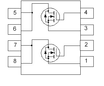
Features: `5.5 A, 20 V. RDS(ON) = 0.035 @ VGS = 4.5 V RDS(ON) = 0.045 @ VGS = 2.7 V.`High density cell design for extremely low RDS(ON).`High power and current handling capability in a widely used surface mount package.`Dual MOSFET in surface mount package.PinoutSpecifications Symbol P...
NDS8926: Features: `5.5 A, 20 V. RDS(ON) = 0.035 @ VGS = 4.5 V RDS(ON) = 0.045 @ VGS = 2.7 V.`High density cell design for extremely low RDS(ON).`High power and current handling capability in a widely used ...
SeekIC Buyer Protection PLUS - newly updated for 2013!
268 Transactions
All payment methods are secure and covered by SeekIC Buyer Protection PLUS.
Symbol |
Parameter |
NDS8926 |
Units | |
VDSS VGSS |
Drain-Source Voltage Gate-Source Voltage |
20 8 5.5 20 2 1.6 1 0.9 -55 to 150 |
V V A W °C | |
ID |
Drain Current - Continuous - Pulsed |
(Note 1a) | ||
PD |
Power Dissipation for Dual Operation | |||
Power Dissipation for Single Operation | (Note 1a) (Note 1b) (Note 1c) | |||
TJ,TSTG | Operating and Storage Temperature Range |
RJA RJC |
Thermal Resistance, Junction-to-Ambient Thermal Resistance, Junction-to-Case |
(Note 1a) (Note 1) | <TD w
These N-Channel enhancement mode power field effect transistors NDS8926 are produced using Fairchild's proprietary, high cell density, DMOS technology. This very high density process is especially tailored to minimize on-state resistance and provide superior switching performance. TheNDS8926 is particularly suited for low voltage applications such as DC motor control and DC/DC conversion where fast switching, low in-line power loss, and resistance to transients are needed.