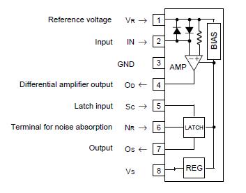
Features: ` Suitable for JIS C 8371` Good temperature characteristics of input sensitivity current` High input sensitivity (VT = 13.5mV Typ.)` Low external component count` High noise and surge-proof` Low power dissipation (Pd = 5mW Typ.) and may be used both as 100V and 200V.` High mounting densi...
M54122L: Features: ` Suitable for JIS C 8371` Good temperature characteristics of input sensitivity current` High input sensitivity (VT = 13.5mV Typ.)` Low external component count` High noise and surge-proo...
SeekIC Buyer Protection PLUS - newly updated for 2013!
268 Transactions
All payment methods are secure and covered by SeekIC Buyer Protection PLUS.
` Suitable for JIS C 8371
` Good temperature characteristics of input sensitivity current
` High input sensitivity (VT = 13.5mV Typ.)
` Low external component count
` High noise and surge-proof
` Low power dissipation (Pd = 5mW Typ.) and may be used both as 100V and 200V.
` High mounting density by SIL package with 8 pins
` Wide temperature range (Ta = -20 +80°C)
Symbol |
Parameter |
Conditions |
Ratings |
Unit |
Is |
Supply voltage |
8 |
mA | |
Is(SG) |
Supply surge current |
(Note 1) |
12 |
mA |
IIN |
Input current |
Between IN and VR (Note 2) |
-250to+250 |
mA |
IIG |
Input pin current |
Between VR and GND, and between IN and GND |
30 |
mA |
VOD |
OD applied voltage |
When external voltage is applied |
6 |
V |
IMA |
MA input current |
When external voltage is applied |
4 |
mA |
VOS |
OS applied voltage |
When external voltage is applied |
6 |
V |
Pd |
Power dissipation |
200 |
mW | |
Topr |
Operating temperature |
-20-80 |
| |
Tstg |
Storage temperature |
-55-125 |
|
Note 1: Current value between VR and IN, and between IN and VR is less than 1ms in the pulse width, and duty cycle is less than 12%. In applying AC current continuously, it is 100mArms in the off-state.
Remarks: GND terminal (pin ) of the circuit is a basis of all the voltages except differential input clamp voltage of DC electrical characteristics, and direction of current is plus (no signal) in flowing into the circuit and is minus ( signal) in flowing out of it. Maximum value and minimum one are shown as absolute value. Please don't apply voltage whose standard is GND terminal in VR and IN pin.