Features: Performance-110/115/120/150 ns Initial Access Speed-125 ns Initial Access Speed (256 Mbit density only)-25 ns Asynchronous Page-Mode Reads-30 ns Asynchronous Page-Mode Reads (256Mbit density only)-32-Byte Write Buffer-6.8 s per byte effective programming time Software-Program and Erase ...
28F640J3: Features: Performance-110/115/120/150 ns Initial Access Speed-125 ns Initial Access Speed (256 Mbit density only)-25 ns Asynchronous Page-Mode Reads-30 ns Asynchronous Page-Mode Reads (256Mbit dens...
SeekIC Buyer Protection PLUS - newly updated for 2013!
268 Transactions
All payment methods are secure and covered by SeekIC Buyer Protection PLUS.
Performance
-110/115/120/150 ns Initial Access Speed
-125 ns Initial Access Speed (256 Mbit density only)
-25 ns Asynchronous Page-Mode Reads
-30 ns Asynchronous Page-Mode Reads (256Mbit density only)
-32-Byte Write Buffer
-6.8 s per byte effective programming time
Software
-Program and Erase suspend support
-Flash Data Integrator (FDI), Common Flash Interface (CFI) Compatible
Security
-128-bit Protection Register
-64-bit Unique Device Identifier
-64-bit User Programmable OTP Cells
-Absolute Protection with VPEN= GND
-Individual Block Locking
-Block Erase/Program Lockout during Power Transitions
Architecture
-Multi-Level Cell Technology: High Density at Low Cost
-High-Density Symmetrical 128-Kbyte Blocks
-256 Mbit (256 Blocks) (0.18m only)
-128 Mbit (128 Blocks)
-64 Mbit (64 Blocks)
-32 Mbit (32 Blocks)
Quality and Reliability
-Operating Temperature:
-40 °C to +85 °C
-100K Minimum Erase Cycles per Block
-0.18 m ETOX™ VII Process (J3C)
-0.25 m ETOX™ VI Process (J3A)
Packaging and Voltage
-56-Lead TSOP Package
-64-Ball Intel® Easy BGA Package
-48-Ball Intel® VF BGA Package (32 and 64 Mbit) (x16 only)
-VCC = 2.7 V to 3.6 V
-VCCQ = 2.7 V to 3.6 V
Parameter | Maximum Rating |
Temperature under Bias Extended | 40 °C to +85 °C |
Storage Temperature | 65 °C to +125 °C |
Voltage On Any signal | 2.0 V to +5.0 V(1) |
Output Short Circuit Current | 100 mA(2) |
NOTES:
1. All specified voltages are with respect to GND. Minimum DC voltage is 0.5 V on input/output signals and 0.2 V on VCC and VPEN signals. During transitions, this level may undershoot to 2.0 V for periods <20 ns. Maximum DC voltage on input/output signals, VCC, and VPEN is VCC +0.5 V which, during transitions, may overshoot to VCC +2.0 V for periods <20 ns.
2. Output shorted for no more than one second. No more than one output shorted at a time.
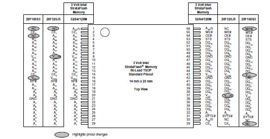
28F640J3 is available in three package types. Each density of the J3C is supported on both 64-ball Easy BGA and 56-lead Thin Small Outline Package (TSOP) packages. A 48-ball VF BGA package is available on 32 and 64Mbit devices. Figure 6, Figure 7, and Figure 8 show the
pinouts.