Circuit Diagram
Index 223
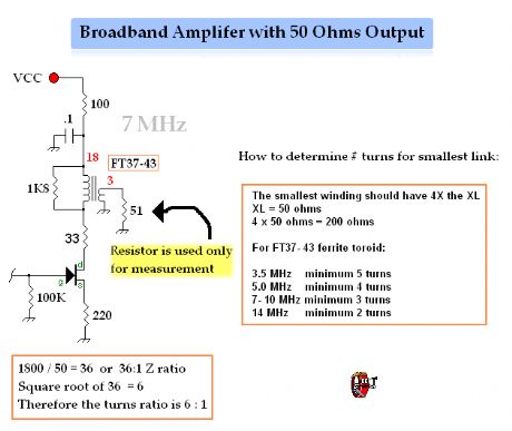
simple amplifier
Published:2012/12/28 0:01:00 Author:muriel | Keyword: simple amplifier
View full Circuit Diagram | Comments | Reading(598)
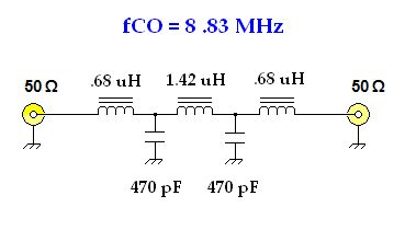
Low-pass Filter 2
Published:2012/12/28 Author:muriel | Keyword: Low-pass Filter
View full Circuit Diagram | Comments | Reading(717)
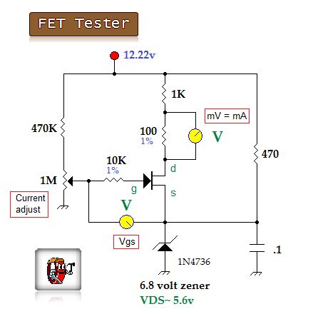
FET Tester 2
Published:2012/12/27 23:59:00 Author:muriel | Keyword: FET Tester
View full Circuit Diagram | Comments | Reading(3302)
FET Tester
Published:2012/12/27 23:59:00 Author:muriel | Keyword: FET Tester
View full Circuit Diagram | Comments | Reading(0)
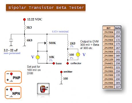
Bipolar Junction Transistor Beta Tester
Published:2012/12/27 23:58:00 Author:muriel | Keyword: Bipolar Junction Transistor, Beta Tester
View full Circuit Diagram | Comments | Reading(2317)
BJT and Diode Matching 2
Published:2012/12/27 23:58:00 Author:muriel | Keyword: BJT and Diode Matching
View full Circuit Diagram | Comments | Reading(1446)
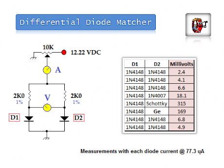
BJT and Diode Matching
Published:2012/12/27 23:57:00 Author:muriel | Keyword: BJT and Diode Matching
View full Circuit Diagram | Comments | Reading(1358)
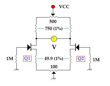
FET Matching 3
Published:2012/12/27 23:57:00 Author:muriel | Keyword: FET Matching
View full Circuit Diagram | Comments | Reading(968)
FET Matching 2
Published:2012/12/27 23:56:00 Author:muriel | Keyword: FET Matching
View full Circuit Diagram | Comments | Reading(1487)
FET Matching
Published:2012/12/27 23:56:00 Author:muriel | Keyword: FET Matching
View full Circuit Diagram | Comments | Reading(1251)
Wide Range L- C Oscillator 2
Published:2012/12/27 23:55:00 Author:muriel | Keyword: Wide Range, L- C Oscillator
View full Circuit Diagram | Comments | Reading(733)
Wide Range L- C Oscillator
Published:2012/12/27 23:54:00 Author:muriel | Keyword: Wide Range, L- C Oscillator
View full Circuit Diagram | Comments | Reading(883)
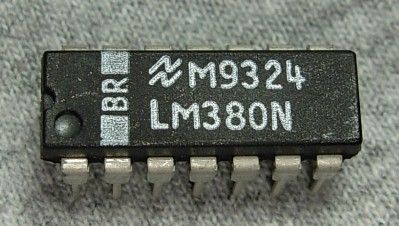
LM380 Power
Published:2012/12/27 23:54:00 Author:muriel | Keyword: LM380, Power
View full Circuit Diagram | Comments | Reading(1311)
10.0 MHz crystal filter 2
Published:2012/12/27 23:53:00 Author:muriel | Keyword: 10.0 MHz, crystal filter
View full Circuit Diagram | Comments | Reading(789)
10 MHz crystal filter
Published:2012/12/27 23:52:00 Author:muriel | Keyword: 10 MHz, crystal filter
View full Circuit Diagram | Comments | Reading(1391)
LM388 audio amplifier and its pin main characteristics
Published:2012/12/27 0:12:00 Author:Ecco | Keyword: audio amplifier, pin main characteristics
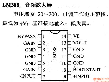
20 to 200 Voltage gain, adjustable operating voltage range,and its lowest bit is 4V; benchmark grounded input; low distortion.
(View)
View full Circuit Diagram | Comments | Reading(1680)
LM6162/6262/6362 operational amplifier and its pin main characteristics
Published:2012/12/27 0:21:00 Author:Ecco | Keyword: operational amplifier , pin main characteristics
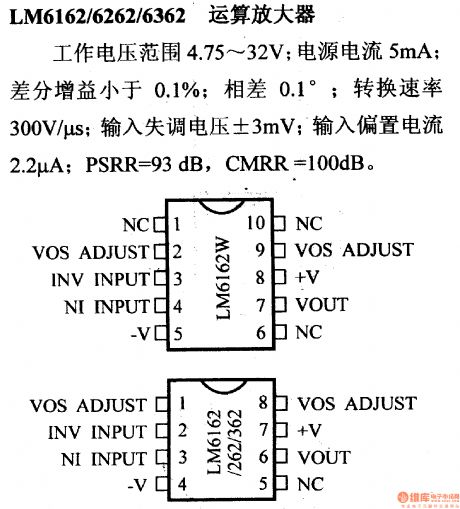
4.75 to 32V operating voltage range; 5mA supply current; differential gain is less than 0.1%; difference is 0.1 °; 300V/μs conversion rate; ±3mV input offset voltage; 2.2 μA input bias current; PSRR = 93dB.CMRR = 100dB.
(View)
View full Circuit Diagram | Comments | Reading(672)
LM709 general purpose operational amplifier and its pin main characteristics
Published:2012/12/27 1:37:00 Author:Ecco | Keyword: general purpose , operational amplifier , pin main characteristics
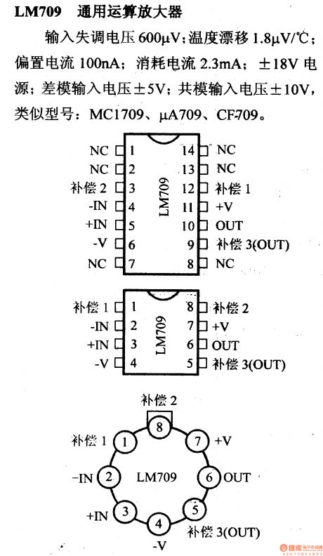
600μV input offset voltage; 1.8μV / ℃ temperature drift; 100nA bias current; 2.3mA current consumption; ± 18V power supply; ± 5V differential-mode input voltage; ± 10V common-mode input voltage. Similar models: MC1709, μA709, CF709.
(View)
View full Circuit Diagram | Comments | Reading(2204)
MA326 high-precision and wideband op amp and its pin main characteristics
Published:2012/12/27 1:28:00 Author:Ecco | Keyword: high-precision , wideband op amp, pin main characteristics
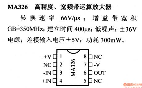
66V/μs conversion rate; Gain Bandwidth Product GB = 350MHz; 400μs settling time; Low Noise; ± 36V power supply; ± 5V differential-mode input voltage; 300mW power consumption.
(View)
View full Circuit Diagram | Comments | Reading(561)
MA336 dual JFET input op amp and its pin main characteristics
Published:2012/12/27 1:33:00 Author:Ecco | Keyword: dual JFET input, op amp , pin main characteristics
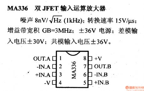
8nV / √ ˉ Hz ( 1kHz) noise; 15V/μs conversion rate; Gain Bandwidth Product GB = 3MHz; ± 36V power supply; differential mode input voltage ± 30V; ± 36V common mode input voltage.
(View)
View full Circuit Diagram | Comments | Reading(587)
| Pages:223/2234 At 20221222223224225226227228229230231232233234235236237238239240Under 20 |
Circuit Categories
power supply circuit
Amplifier Circuit
Basic Circuit
LED and Light Circuit
Sensor Circuit
Signal Processing
Electrical Equipment Circuit
Control Circuit
Remote Control Circuit
A/D-D/A Converter Circuit
Audio Circuit
Measuring and Test Circuit
Communication Circuit
Computer-Related Circuit
555 Circuit
Automotive Circuit
Repairing Circuit
