Circuit Diagram
Index 2003
crystal diode DDZX22DTS、DDZX24CTS、DDZX43TS internal circuit diagram
Published:2011/4/26 10:32:00 Author:Nancy | Keyword: crystal diode
View full Circuit Diagram | Comments | Reading(317)
crystal diode DDZX16CTS、DDZX18CTS、DDZX20DTS internal circuit diagram
Published:2011/4/26 10:34:00 Author:Nancy | Keyword: crystal diode
View full Circuit Diagram | Comments | Reading(346)
BZMTA-700/800 amplifier control and display circuit diagram (-)
Published:2011/4/26 10:38:00 Author:Nancy | Keyword: amplifier, control and display

(View)
View full Circuit Diagram | Comments | Reading(434)
crystal diode DDZX13BTS、DDZX14TS、DDZX15TS internal circuit diagram
Published:2011/4/26 10:41:00 Author:Nancy | Keyword: crystal diode
View full Circuit Diagram | Comments | Reading(421)
Gaoshi AV9095 amplifier key and display circuit diagram
Published:2011/4/26 10:47:00 Author:Nancy | Keyword: Gaoshi, amplifier, key and display

(View)
View full Circuit Diagram | Comments | Reading(579)
Gaoshi AV9095 amplifier key and display circuit diagram (-)
Published:2011/4/26 10:46:00 Author:Nancy | Keyword: Gaoshi, amplifier, key and display

(View)
View full Circuit Diagram | Comments | Reading(578)
555 square wave generator circuit diagram
Published:2011/4/26 10:48:00 Author:Nancy | Keyword: square wave, generator
View full Circuit Diagram | Comments | Reading(1188)
Gaoshi AV9092B amplifier display and control circuit diagram
Published:2011/4/26 10:50:00 Author:Nancy | Keyword: Gaoshi, amplifier, display and control

(View)
View full Circuit Diagram | Comments | Reading(377)
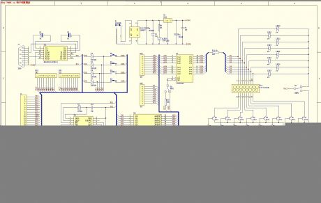
A professional 51 MCU test panel
Published:2011/4/26 3:51:00 Author:Ecco | Keyword: professional , MCU , test panel


Onboard buzzer and reset button can be used to do some sound tests. Board four button inputs can be selectable interrupt / query. All four ports are connected to P can be pre-10K pull-up resistor row. IIC bus is connected real-time clock device PCF8563. IIC bus is connected to EEPROM device 24C02, the features are similar to the Hengjian's products. 74LS244 onboard driver chips can be driven by non-simple P port directly, it has better protection to single chip. MAX232 chip board ahs standard RS-232-C serial interface and it can be used for online testing for PC.
(View)
View full Circuit Diagram | Comments | Reading(915)
74 series digital circuit 74LS280 74S280 and other 9 bits odd even generator/validator
Published:2011/4/26 4:32:00 Author:May | Keyword: digital, 9 bits, odd even generator, validator
View full Circuit Diagram | Comments | Reading(741)
Electronic fishing device
Published:2011/4/26 3:42:00 Author:May | Keyword: Electronic, fishing device
View full Circuit Diagram | Comments | Reading(1235)
1500W square-wave inverter
Published:2011/4/26 3:43:00 Author:May | Keyword: 1500W, square-wave inverter
View full Circuit Diagram | Comments | Reading(1712)
74 series digital circuit 74LS445 BCD decimal decoder/driver (OC)
Published:2011/4/26 3:57:00 Author:May | Keyword: digital, BCD, decimal decoder, driver, OC

74 series digital circuit 74LS445 BCD decimal decoder/driver (OC)
74LS145's low voltage type, withstand voltage is 7V; absorption current is 80mA.; typical power consumption is 35mW; Pin diagram and function table is same to 74LS145. (View)
View full Circuit Diagram | Comments | Reading(2273)
74 series digital circuit 74LS448 four three bus receiver (OC)
Published:2011/4/26 3:59:00 Author:May | Keyword: digital, four three bus receiver, OC

Its pin diagram and function table is same as 74LS440. (View)
View full Circuit Diagram | Comments | Reading(635)
74 series digital circuit 74490 74LS490 etc dual four bit decade counter
Published:2011/4/26 4:07:00 Author:May | Keyword: digital, dual four bit, decade counter

74490, 74LS490, 74HC490 dual four bit decade counter
It is the dual type of 7490A and 74LS90 normal counter. The highest counter frequency is 35MHz. It is buffer output. (View)
View full Circuit Diagram | Comments | Reading(2552)
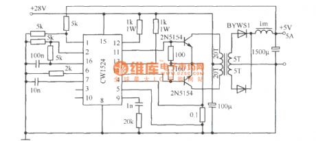
Push pull type switching regulated power supply circuit composed of CW1524
Published:2011/4/26 3:45:00 Author:May | Keyword: Push pull, switching regulated power supply
View full Circuit Diagram | Comments | Reading(612)
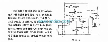
SIPMOS transistor push pull control circuit
Published:2011/4/26 2:56:00 Author:May | Keyword: SIPMOS transistor, push pull control

Input end of this circuit is connected integrated circuit TDA4700. When its output transistor turns on, base of T1 has voltage which is determined by R1, R2. Diode D1 and D2 is used to prevent the over saturation of T1. If output transistor of TDA4700 is cut off, T1 is cut off, T2 is controlled by R4, at this time, SIPMOS transistor input capacitor (crossover in the justified of R5 and T2) is as limiting resistor. The current consume of this circuit is very small because it adopts push pull control mode. (View)
View full Circuit Diagram | Comments | Reading(560)
RS232C Pin with the diagonal connections
Published:2011/4/26 3:36:00 Author:Ecco | Keyword: Pin , diagonal , connections
View full Circuit Diagram | Comments | Reading(533)
Simple nickel-cadmium battery charger
Published:2011/4/25 23:02:00 Author:May | Keyword: Simple, nickel-cadmium, battery charger
The circuit is shown in diagram 2-2. It consists of three terminal regulator 708 and four loads current source composed of triode VT2~VT5. VT1 and corresponding adjustable resistance RRP1, RP2 and switching tube S is used to control each roads charging current. When S is placed on position 1, charging current of each roads is 90mA; when S placed 2 and 3, it can get 100mA~300mA charging current by adjusting RP1 and RP2. If it adopts current above 200mA to charge, each triode should add radiator. Light emitting diode VD5~VD8 in diagram 2-2 is used as charge indicator. Whole circuit can supply by 220V mains, it also can supply by 12V storage battery. Charge time can count according to the following formula:
Charging time(h)=Nickel-cadmium battery capacity(mAh)/charge current(mA)
In actual use, charging time can proper extended.
(View)
View full Circuit Diagram | Comments | Reading(1307)
Compact keyboard trainer-the application example of PS / 2 keyboard interface circuit
Published:2011/4/26 3:33:00 Author:Ecco | Keyword: Compact, keyboard trainer, application example , PS / 2, keyboard interface
View full Circuit Diagram | Comments | Reading(451)
| Pages:2003/2234 At 2020012002200320042005200620072008200920102011201220132014201520162017201820192020Under 20 |
Circuit Categories
power supply circuit
Amplifier Circuit
Basic Circuit
LED and Light Circuit
Sensor Circuit
Signal Processing
Electrical Equipment Circuit
Control Circuit
Remote Control Circuit
A/D-D/A Converter Circuit
Audio Circuit
Measuring and Test Circuit
Communication Circuit
Computer-Related Circuit
555 Circuit
Automotive Circuit
Repairing Circuit


