
Circuit Diagram
Index 1285
CLOCK_RADIO
Published:2009/6/26 3:14:00 Author:May

View full Circuit Diagram | Comments | Reading(783)
VARICAP_TUNED_FET_DIP_METER_WITH_1_kHz_MODULATION
Published:2009/6/26 3:07:00 Author:May

View full Circuit Diagram | Comments | Reading(1227)
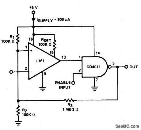
RAMP_GENERATOR_WITH_VARIABLE_RESET_LEVEL
Published:2009/6/26 3:05:00 Author:May

View full Circuit Diagram | Comments | Reading(0)
PRECISION_RAMP_GENERATOR
Published:2009/6/26 3:05:00 Author:May
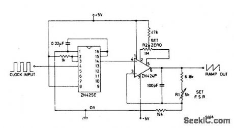
View full Circuit Diagram | Comments | Reading(580)
DIP_MEITR_USING
Published:2009/6/26 3:04:00 Author:May

Circuit NotesGate 2 is used to adjust the oscillation level. (View)
View full Circuit Diagram | Comments | Reading(671)
VLF_CONVERTER
Published:2009/6/26 3:51:00 Author:Jessie

This converter uses a low-pass filter instead of the usual tuned circuit so the only tuning required is with the receiver. The dual-gate MOSFET and FET used in the mixer and oscillator aren't critical. Any crystal having a frequency compatible with the receiver tuning range may be used. For example, with a 3500 kHz crystal, 3500 kHz on the receiver dial corresponds to zero kHz; 3600 to 100 kHz; 3700 to 200 kHz, etc. (At 3500 khz on the receiver all one can hear is the converter os-cillator, and VLF signals start to come in about 20 kHz higher.) (View)
View full Circuit Diagram | Comments | Reading(1)
NEON_LAMP_DRIVER_FOR_5_TO_15_V_SUPPLIES
Published:2009/6/26 3:51:00 Author:Jessie

This neon-lamp driver based on the 555 T1 can be wound on an old TV flyback transformer core. (View)
View full Circuit Diagram | Comments | Reading(3568)
SQUELCH_CIRCUIT_FOR_AM_OR_FM
Published:2009/6/26 3:50:00 Author:Jessie

View full Circuit Diagram | Comments | Reading(959)
CURRENT_LIMITING_REGULATOR
Published:2009/6/26 3:49:00 Author:Jessie

Floating adjustable regulators can be used as current Iimiters. Resistor R1 programs the current flowing through R2. (View)
View full Circuit Diagram | Comments | Reading(937)
MULTIVOLTAGE_POWER_SUPPLY
Published:2009/6/26 3:49:00 Author:Jessie

This dual-polarity, multivoltage power supply can be built for a very small investment. The circuit is built around 78XX and 79XX series 1-A voltage regulators, four 3-A diodes, a 24-30-V 2-6-A transformer, and eight filter capacitors. (View)
View full Circuit Diagram | Comments | Reading(1932)
UNIVERSAL_MOTOR_SPEED_CONTROL
Published:2009/6/26 3:46:00 Author:Jessie

The resistor capacitor network R1-R2-C1 provides a ramop-type reference voltage superimposed on top of a dc volatage adjustable with the speed-setting potentiometer R2.This reference voltage appearing at the wiper of R2 is balanced against the residual counter emf of the motor through the SCR gate.As the motor slows down due to heavy loading,its couter emf falls,and the reference ramp triggers the SCR earlier in the ac cycle.More voltage is thereby applied to the motor causing it to pick up speed again.Performance with the C106 SCR is particularly good because the low trigger current requirements of this device allow use of a flat top reference voltage, which provides good feedback gain and close speed regulation. (View)
View full Circuit Diagram | Comments | Reading(2469)
CMOS_LINE_RECEIVER
Published:2009/6/26 3:45:00 Author:Jessie
The trip point is set half way between the supplies by R1 and R2; R3 provides over 200 mV of hysteresis to increase noise immunity.Maximum frequency of operation is about 300 kHz. If response to TTL levels is desired, change R2 to 39 K. The trip point is now cen-tered at 1.4 V. (View)
View full Circuit Diagram | Comments | Reading(1612)
SIMPLE_LF_CONVERTER
Published:2009/6/26 3:44:00 Author:Jessie

This converter allows coverage from 25 kHz up to 500 kHz. Use short coax from the converter to receiver antenna input. Tune the receiver to 3.5 MHz, peak for loudest crystal calibrator and tune your receiver higher in frequency to 3.6 MHz and you're tuning the 100 kHz range. 3.7 MHz puts you at 200 kHz, 3.8 MHz equals 300 kHz, 3.9 MHz yields 500 kHz, and 4.0 MHz gives you 500 kHz. (View)
View full Circuit Diagram | Comments | Reading(1350)
INVERTING_POWER_SUPPLY
Published:2009/6/26 3:43:00 Author:Jessie

This circuit will provide a negative dc voltage that is approximately equal to the positive input voltage at no load and about 3 V less at 10 mA load. VIN is from +5 to +15 Vdc, Do not exceed 15 V or U1 might be damaged. (View)
View full Circuit Diagram | Comments | Reading(663)
FM_RADIO
Published:2009/6/26 3:43:00 Author:Jessie
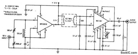
View full Circuit Diagram | Comments | Reading(1211)
ANALOG_RECEIVER_LOW_TEMPERATURE_DRIFT
Published:2009/6/26 3:41:00 Author:Jessie

View full Circuit Diagram | Comments | Reading(983)
SIMPLE_NEGATIVE_SUPPLY_FOR_LOW_CURRENT_APPLICATIONS
Published:2009/6/26 3:41:00 Author:Jessie

This dc negative-voltage generator based on the 555 produces a negative output voltage equal to approximately 2x the dc supply voltage. (View)
View full Circuit Diagram | Comments | Reading(1095)
TRANSMATCH
Published:2009/6/26 3:04:00 Author:Jessie

Tapped variable inductance and titree broadcast tuning capacitors are easily preadjusted to match low-power (QRP) transmitter to antenna for SWR of 1 in commonly used amateur bands. Resistance bridge is used only for initial determination of correct settings for C1, C2, C3, and S2 at each band to be used.Set S1 at n, feed peak output of transmitter to J1 (5 W maximum), and adjust R4 for full.scale frequency to be used. Repeat procedure with reading of M1. Next, conned 50.ohm resistive antenna or feed line in place of dummy load, load between CR1-R1 junction and ground. Meter reading should now drop to zero, indicating null at 50 ohms,Move 50-ohm dummy load to J2, set S1 at 2, and adjust seetings of C1,C2, and C3 for zero deflection of meter,Note settings, then repeat for each other transmitter frequency to be used. Repeat procedure with antenna or feed line in place of dummy load, After completing adjustments, set S1 to 3 to bypass bridge for normal transmitter opetation.-D. DeMaw, A Poor Ham's QRP Transmatch, QST, Oct. 1973, p 11,13. (View)
View full Circuit Diagram | Comments | Reading(2773)
LINEAR_VOLTAGE_RAMP_GENERATOR
Published:2009/6/26 3:03:00 Author:Jessie


In the monostable mode, the resistor can be replaced by a constant current source to provide a linear ramp voltage. The capacitor still charges from 0 to 2/3 Vcc. The linear ramp time is given by the following equation:If VB is much larger than VBE, then t can be made independent of Vcc. (View)
View full Circuit Diagram | Comments | Reading(686)
1_kHz_MODULATOR_FOR_VHF_SOURCE
Published:2009/6/26 3:02:00 Author:Jessie

Used with 144-MHz signal generator driving VSWR bridge, for measuring and matching VHF antennas. R1 adjusts frequency of NE555 timer used in place of customary MVBR. Series-pass transistor increases output of MVBR about 2 dB.-J. Reisert, Matching Techniques for VHF/UHF Antennas, Ham Fladio, July 1976, p 50-56. (View)
View full Circuit Diagram | Comments | Reading(1060)
| Pages:1285/2234 At 2012811282128312841285128612871288128912901291129212931294129512961297129812991300Under 20 |
Circuit Categories
power supply circuit
Amplifier Circuit
Basic Circuit
LED and Light Circuit
Sensor Circuit
Signal Processing
Electrical Equipment Circuit
Control Circuit
Remote Control Circuit
A/D-D/A Converter Circuit
Audio Circuit
Measuring and Test Circuit
Communication Circuit
Computer-Related Circuit
555 Circuit
Automotive Circuit
Repairing Circuit