
power supply circuit
Index 96
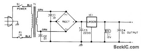
15_V_AT_600_mA
Published:2009/7/17 2:13:00 Author:Jessie

Developed for 2-meter FM transceiver used as repeater. Output voltage is well filtered. Regulator allows voltage to drop only 0.1 V when repeater goes from standby to transmit. Use heatsink on 2N3055 series-regulator transistor.-H. Cone, The Minirepeater, 73 Magazine, June 1975, p 55-57, 60-62, and 64-65. (View)
View full Circuit Diagram | Comments | Reading(1035)
CEMENT_SETTING_TIMER
Published:2009/7/17 2:11:00 Author:Jessie

Sample of cement is inserted as dielectric material in test-tube capacitor, and admittance readings are made every 15 minutes using 7-Mc crystal oscillator with anode circuit tuned to 28Mc.Maximum admittance indicates end of setting process.-J. M. Tobio, Electronics Determines Cement Setting Time, Electronics, 31:41, p 88-90. (View)
View full Circuit Diagram | Comments | Reading(687)
ECHO_SYSTEM_DYNAMIC_RANGE_BOOSTER
Published:2009/7/17 2:10:00 Author:Jessie

Using a variable-gain preamplifier helps improve the dynamic range of echo systems. Here, Harris Semiconductor's HA2556 multiplier is used to implement the variable-gain preamplifier and establish the signal bandwidth and noise figure. An echo sys-tem with a fixed-gain preamplifier exhibits poor dynamic range because close targets (long return times) have high signal amplitudes, whereas distant targets (long return times) produce amplitudes that are much lower. One solution involves a preamplifier that has a gain that is proportional to time so that the gain witl be small for close targets and large for dislant targets. The preamplifier must meet all of the other preamplifier criteria, such as bandwidth and noise performance. Moreover, the added time-dependent gain function must not degrade the signal. This type of variable-gain preamplifier can be built with a multiplier IC, the Harris Semiconductor HA2556. This IC establishes the signal bandwidth and noise figure because it is the only component in the signal path. The HA5177 op amp and its associated circuitry make up a constant-current source with a current (I) of VD1/R2=51μA. If the switch (S1) is in the LINEAR-position with Q2's gate held high, the cur-rent source is shorted to ground by Q2 and the multiplier gain is set to zero. When the transmission of the outgoing signal is complete, Q2's gate is brought low, forcing it into a very high drain resistance state (almost an open circuit). Consequently, the HA5177 current can charge C1 in a linear manner. The voltage across 01 then ramps up from 0 to 5V in 1 ms. During the first portion of the ramp, when the returned signal is very large, the multiplier gain is small because VX, is small. As time increases, so does VX providing more gain through the multiplier as the expected echo decreases in amplitude. As a result, the output-voltage swing of the multiplier tends to stay constant for large changes in input signal. In addition, the dynamic range is improved to the amount of the ramp change, which is more than 60 dB with the values shown in the figure. (View)
View full Circuit Diagram | Comments | Reading(1418)
STEPPED_WAVEFORM_GENERATOR
Published:2009/7/17 2:08:00 Author:Jessie

A decode counter(U2) is used to perform sequential switching vla a CD 4066.Analog switch is togenerate a waveform. The clock is a 567 PLL or otherVCO chip. (View)
View full Circuit Diagram | Comments | Reading(1519)
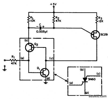
COMMON_EMITTER_BETA_TEST_SET
Published:2009/7/17 2:08:00 Author:Jessie

Switch permits testing both npn and pnp transistors over wide current and voltage ranges. Two feedback amplifiers are used, one for npn and the other for for pnp.-R . M. Mann, Fresh Approach to Measuring Transistor Beta Electronics,36:30,p 47-49 (View)
View full Circuit Diagram | Comments | Reading(684)
SAWTOOTH_GENERATOR_FOR_SWEEP_GENERATORS
Published:2009/7/17 2:07:00 Author:Jessie

This circuit will generate a linear sawtooth between 30 Hz and 3000 Hz. Q1 is a constant-current source that charges C1 until the output level at Q3 emitter triggers U1A and U1B, which turns on Q4 and discharges C1. The frequency range can be varied by changing the value of C1. This circuit should be good to several tens of kHz.
(View)
View full Circuit Diagram | Comments | Reading(766)
RAMP_GENERATOR
Published:2009/7/17 2:06:00 Author:Jessie

Providing a 0-to 10-V excurslon from 0.4 Hz to 100 kHz,this circuit offers both simplicity and smallslze.The negative current through R1 produces the ramp's positive slope and causes the output of IC1 to increase linearly toward the+15-V rail. (View)
View full Circuit Diagram | Comments | Reading(2532)
SIMPLE_STAIRCASE_GENERATOR
Published:2009/7/17 2:05:00 Author:Jessie

U2 is a decade counter /divider. U1 is used as a switch debouncer. For a self-generating system, connect a resistor between pins 2 and 3 of a U1 value that should be between 10 kΩ and several MΩ, depending on desired frequency. C1 can also be varied to change frequency. Also, S1 can be omitted in the self-generating version. (View)
View full Circuit Diagram | Comments | Reading(2257)
DIGITAL_SAWTOOTH_GENERATOR
Published:2009/7/17 2:04:00 Author:Jessie
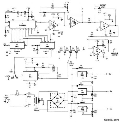
This straightforward circuit uses an NE555 timer as an oscillator, a 7493 counter chain and a DAC0806 D/A converter. The counter output feeds the DAC, producing a linearly increasing voltage, which drives an op amp and a dc-level insertion circuit. The clock frequency must be 256 times the desired sawtooth output frequency.
(View)
View full Circuit Diagram | Comments | Reading(2016)
STRAY_CAPACITANCE_CANCELLATION_TECHNIQUE
Published:2009/7/17 2:03:00 Author:Jessie
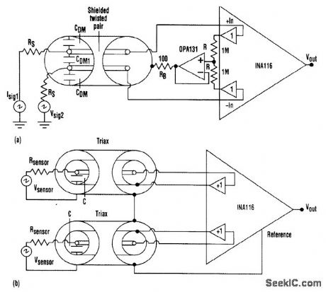
A shielded twisted-pair cable eliminates common-mode capacitance, but the differential capacitance remains (a). A triax cable eliminates both common-mode and differential capacitances (b). (View)
View full Circuit Diagram | Comments | Reading(751)
R_C_DIRECTIONAL_COUPLER
Published:2009/7/17 2:03:00 Author:Jessie
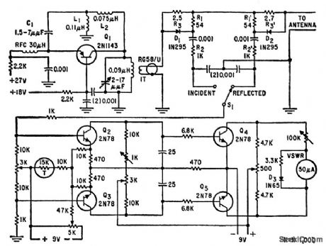
Couples variable-frequency 150-175 Mc oscillator to vhf antenna and furnishes incident and reflected power samples to d-c amplifier for measuring voltage-standing wave ratio.-J. Hanson, Unconventional Technique for Measuring VSWR, Electronics, 32:43, p 120-121. (View)
View full Circuit Diagram | Comments | Reading(675)
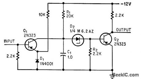
_12_V_AT_50_mA
Published:2009/7/17 2:02:00 Author:Jessie
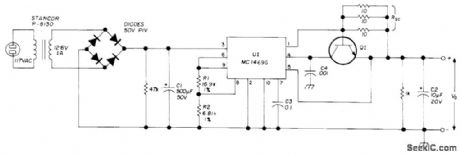
Provides 0.1% regulation as required for PLL RTTY tuning unit and other critical applications. RSC and Q1 provide short-circuit protection for regulator.When output current reaches about 200 mA, Q1 turns on and limits regulator output. U1 can be Motorola MC1469G or HEP C6049G, and at is any general-purpose NPN silicon transistor.-E. Law-rence, Precision Voltage Supply for Phase-Locked Terminal Unit, Ham Radio, July 1974, p 60-61. (View)
View full Circuit Diagram | Comments | Reading(602)
SELF_RESETTING_PULSE_STRETCHER
Published:2009/7/17 2:00:00 Author:Jessie
Produces output pulse that lasts for designated period of time after last of group of 20-microsec 5.v input pulses disappears. Circuit then resets, and draws no current while quiescent. Amount of stretching is determined by charging of C through R2, and is 55 microsec for values shown. Gate-turnoff scr can be used in smith, self-Resetting Pulse Stretcher, EEE, 12:8, p 71-72. (View)
View full Circuit Diagram | Comments | Reading(536)
CUTTING_NOISE_PICKUP_WITH_REMOTE_GAIN
Published:2009/7/17 2:00:00 Author:Jessie
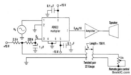
At times, gain control that is remote from the amplifier and speaker is required. However, merely extracting the gain-control potentiometer from a typical amplifier and placing it remotely will contaminate the signal with pickup. One simple solution is to use an analog multiplier as a gain-control element. The 2.5-kΩ resistor and the remote gain-control potentiometer form an attenuator of the +15-V supply, whose output is filtered through a low-pass RC filter. The resistance of the twisted pair of leads is negligible compared with the potentiometer's 5-kΩ resistance. When the remote gain-control potentiometer is at maxim Um resistance, the control voltage, Ec,at pin 3 of the multiplier is at a nominal value of + 10 Vdc. This results in a maximum input amplitude to the amplifier, which is equal to the original input signal es Correspondingly, when the gain-control potentiometer is set to zero resistance, the signal input to the amplifier is nominally zero. Any ac signals that might be picked up by the long run of wire are effectively attenuated by the large time constant of the low-pass filter. (View)
View full Circuit Diagram | Comments | Reading(620)
12_V_FOR_TRANSCEIVER_1
Published:2009/7/17 2:00:00 Author:Jessie
Output voltage varies only 0.2 V between transmit and receive. Transistor can be mounted directly on side of metal minibox for heatsinking. Transformer secondary is 24 V at 5 A. - Circuits, 73 Magazine, March 1977, p 152. (View)
View full Circuit Diagram | Comments | Reading(516)
DELAY_LINE_PULSE_SHAPER
Published:2009/7/17 1:59:00 Author:Jessie
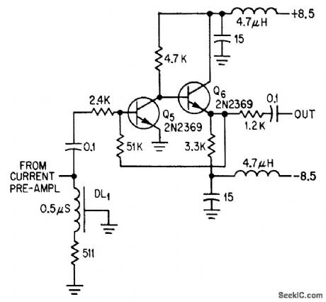
Voltage pulse from current preamplifier of multiplier photo-tube is shaped by DL1, which is shorted at one end and terminated at other end with ifs characteristic impedance, to normalize input pulse width at twice 0.5-microsec characteristic delay of line. First stage gives open-loop gain of 118. Second stage gives low-impedance drive for feedback and for following discriminator amplifier. Total loop gain is 17 for bandwidth of1 Mc.-R. Cuikay and T. Callahan, Orbiting Observatory to Measure Stars' Dim Light, Electronics, 379, p 28-31. (View)
View full Circuit Diagram | Comments | Reading(758)
5_V_AT_1_A_1
Published:2009/7/17 1:58:00 Author:Jessie
Simple lab supply provides voltage required for digital ICs Rectifier is 6-A 50-PIV bridge. Power transformer has 12.6-V secondary rated 1 A, such as filament transformer. -G. McClellan, Give That Professional Look to Your Home Brew Equipment, 73 Magazine, Feb. 1977, p 28-31. (View)
View full Circuit Diagram | Comments | Reading(553)
ZENER_DIODE_PULSE_STRETCHER
Published:2009/7/17 1:57:00 Author:Jessie
Gives delays up to 50 millisec without need for large capacitance values, by varying R1; delay is 10 millisec for 20K value shown. Input is negative 1-millisec pulse, which is stretched by amount of delay.-A. S. Robin-son, Zener Diode Allows Delay Without Large Capacitors, Electronics, 39:11, p 93. (View)
View full Circuit Diagram | Comments | Reading(1080)
MAGAMP_REGULATES_2300_V_SUPPLY
Published:2009/7/17 1:56:00 Author:Jessie
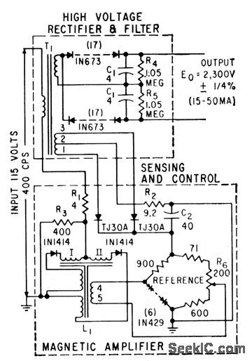
Self-saturating magnetic amplifier is placed on low-voltage input side of high-voltage 400-cps rectifier and auxiliary winding is added for output sensing, to isolate control and sensing functions from high-voltage circuit.-W. J. McDaniel and T. L. Tanner, Regulating High Voltage with Magnetic Amplifiers, Electronics, 32:29, p 64. (View)
View full Circuit Diagram | Comments | Reading(909)
WIRELESS_DC_PROBE
Published:2009/7/17 1:55:00 Author:Jessie
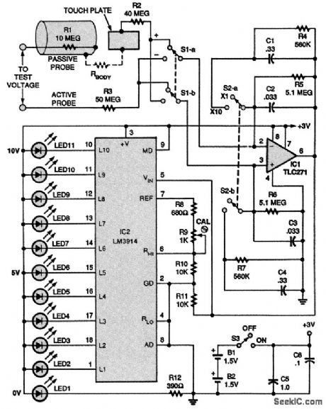
This probe for low voltages only (<100 V) uses the body to complete the dc circuit in a novel way. The schematic for the dc voltmeter is shown. Power for the circuit is provided by two 1.5-V N-type cells, B1 and B2, which are wired in series. For the circuit to work, it must be completed or closed. That is accomplished when the passive probe is held in one hand and the active probe is held in the other and the points of the two probes are placed across two points in a circuit under test. The resistor labeled Rbody is simply the resistance of the user's body. For Rbody to be swamped out, or kept from interfering with the reading, extremely high input-circuit impedances are used in the circuit. All of the people tested by the author for this project indicated a body resistance from hand to hand in the range of 200,000 to 500,000 Ω. Therefore, an input impedance of 50 MΩ, resistor R3, was added. That also provided an adequate safety isolation feature. The reduction of RFI and 60-Hz pickup is accomplished by the use of a symmetrical difference amplifier (IC1) at the input; the inherent common-mode rejection takes care of most the ac-related problems. The amplifier used for IC1 is a TLC271 CMOS op amp. Switch S1 is used to select polarity. Note that 50 MΩ of resistance are present at both of IC1's differential inputs (R3 at one input and the combined series resistance of R1 and R2 at the other). The user is placed in series with the 100-MΩ loop containing a 10-MΩ resistor (R1) as the protective device in the passive-probe section. Capacitors C1 to C4 provide additional filtering of residual ac noise and allow IC2, an LM3914 bar-graph display driver, to step up sequentially. Switch S2 selects between two selectable input ranges: XI, where each step equals 1 V, and X10, where each step equals 10 V. The display is made up of LED1 to LED11; LED2 through LED11 indicate the individual steps. LED1, the 0-V indicator, is also the power-on indicator. (View)
View full Circuit Diagram | Comments | Reading(1310)
| Pages:96/291 At 2081828384858687888990919293949596979899100Under 20 |
Circuit Categories
power supply circuit
Amplifier Circuit
Basic Circuit
LED and Light Circuit
Sensor Circuit
Signal Processing
Electrical Equipment Circuit
Control Circuit
Remote Control Circuit
A/D-D/A Converter Circuit
Audio Circuit
Measuring and Test Circuit
Communication Circuit
Computer-Related Circuit
555 Circuit
Automotive Circuit
Repairing Circuit