
Control Circuit
Index 150
GAME_FEEDER_CONTROLLER
Published:2009/7/1 21:04:00 Author:May
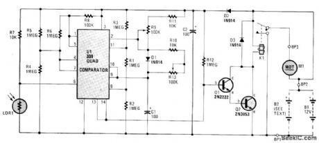
The circuit is built around an LM339 quad comparator, U1, which forms the basis of a Schmitt trigger, timer circuit, and a window comparator. One comparator within the LM339 (pins 1, 7, 6), plus LDR1, R4, R5, R6 and R8, is used as a Schmitt trigger.The timer circuit (which receives its input from the Schmitt trigger) consists of R9, R10, R11, R13. The last two-fourth's of U1 (pins 8, 9, 10, 11, 13 and 14) are wired as a window comparator. The two inputs to the window comparator are derived from the charge on capacitor C1-which is fed to pins 9 and 10 of U1. The other inputs are picked from two points along a voltage-divider network, consisting of R1, R2, and R3. Diode D1 is used as a blocking diode, forcing capacitor C1 to discharge through R10 and R13.The window comparator looks for any voltage falling between one-third and two-thirds of the supply voltage. When the voltage falls between those two points, the output of the window comparator (pins 13/14) goes high. Transistors Q1, and Q2 are turned on, when the pins 13/14 junction goes high, energizing the relay, K1. The energized relay provides a dc path to ground, activating the motor, Ml, which reloads the feeder. The timer circuit also provides immunity from triggering, due to lightning. The on-time of relay K1 is determined by the charge cycle of C1, R11, and R9 or the discharge cycle of C1, R10, and R13. Changing the value of either a resistor or the capacitor, changes the timing cycle. (View)
View full Circuit Diagram | Comments | Reading(3320)
ENLARGER_TIMER
Published:2009/7/24 3:24:00 Author:Jessie

This fairly accurate design is also suitable for color work. Unlike many simple timer designs, this unit is based around the LM3905N 8-pin D.I.L. precision timer IC, which repeats the timing period very consistently with little drift, although the accuracy of the timer depends on the tolerance of the components used. In the circuit diagram, IC1 is an LM3905N timer whose period is determined by an external RC network selected by switches S1 and S2. The formula for the time period is t=RC, where t is in seconds, R is in ohms, and C is in farads. Switch S1 is a single-pole, 12-way rotary type which selects among timing resistors R1 to R11. S2 is a three-pole, four-way rotary switch that progressively adds C1 to C3 in parallel with C4, thereby adjusting the timing capacitance range. In conjunction with the 1-percent resistor network (R1 to R11), each lμ/1M pair represents a 1-s period; hence, the maximum possible period is 44 s. Timing is initiated by closing switch S3. A floating output transistor within IC1 drives a PNP buffer, which, in turn, operates relay RLA. The circuit requires roughly a 12-V rail, and the relay coil is chosen accordingly. The IC will operate from 4.5 to 40 Vdc, and a standard full-wave power supply can be used. The relay contacts RLA1 switch on the enlarger bulb, and a separate FOCUS switch (S5) can be included across the relay contacts (or perhaps drive the relay coil manually), if desired. (View)
View full Circuit Diagram | Comments | Reading(4347)
PUSH_ON_PUSH_OFF_ELECTRONIC_SWITCH
Published:2009/7/1 21:01:00 Author:May

Transistors Q1 and Q2 make up the flip-flop while Q3 drives a reed relay. When powe is first applied to the circuit, Q1 and Q3 are conducting and Q2 is cut off.Momentarily closing S1 causes the flip-flop to switch states-Q1 cuts off and Q2 conducts.When Q2 is conducting, its collector drops to around 0.6 volt. That prevents base current from flowing into Q3 so it is cut off, de-energizing relay K1. The flip-flop changes state every time S1 is pressed. Capacitors C1 and C2 ensure that Q1 is always the transistor that turns on when power is first applied to the circuit. When power is first applied to the basic flip-flop, the initial status is random-Q1 and Q2 both try to conduct and, usually, the transistor with the higher gain will take control, reaching full conduction and cutting off the other one. However, differences in the values of the collector and coupling resistors will also influence the initial state at power-on. With C2 in the circuit, it and R4 form an R-C network that slightly delays the rise in Q2's base voltage. That glves Q1 sufficient time to reach saturation and thus take control. (View)
View full Circuit Diagram | Comments | Reading(6280)
SPEED_SWITCH
Published:2009/7/1 21:01:00 Author:May

National LM2907 tachometer IC is used as switch to energize load when input frequency exceeds value corresponding to predetermined speed limit. Automotive applications include use as overspeed warning that activates audible and/or visual indicator when auto speed exceeds legal limit or other desiredvalue. Another application is increasing intensity of auto or taxi horn above predetermined speed such as 45 mph. Input is variable-reluctance magnetic pickup positioned against teeth of gear wheel; in typical setup, pickup output is 16.6 Hz at 60 mph. Values shown for comparator-controlling components R1 and C1 (below IC) give switching operation at about 16.6 Hz at input. Report gives design procedure for other frequencies.- Linear Applications, Vol. 2, National Semiconductor, Santa Clara, CA, 1976, AN-162, p 8. (View)
View full Circuit Diagram | Comments | Reading(0)
0_to_100℃_025℃_accurctte_thermistor_based_temperature_measurement
Published:2009/7/24 3:16:00 Author:Jessie
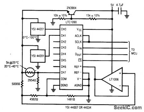
Fig. 13-45 This circuit is an 8-channel, 0 to 100℃, temperature-measurement system, with 0.1℃ resolution. The YSI thermilinear components are measured directly. Accuracy is limited by the sensor repeatability and precision resistors to 0.25℃. Linear Technology Linear Applications Handbook 1990 p DN5-2.
(View)
View full Circuit Diagram | Comments | Reading(489)
AUTOMATIC_REMOTE_RHYTHM_CONTROL
Published:2009/7/1 20:52:00 Author:May
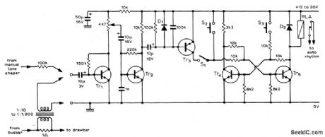
When added to electronic organ,circuitis activated by audio signal from lower manual or pedal, to initiate start of rhythm accompaniment. High-impedance input conhection through 100K ts made to toneshaper output, and transformer connection is used with electromechanical Hammond organ. Transistorand diode types are not critical. If S1 is closed, current passes through to Tr5 and triggers bistable that pulls in relay,S2 and S3 are usedfor manualstart and stop of rhythm.-κ .B.Sorensen.Touch Startof Automatic Rhythm Device,Wireless World.Oct.1974.p381. (View)
View full Circuit Diagram | Comments | Reading(518)
_55_to__125℃_thermometer_using_silicon_sensors
Published:2009/7/24 3:17:00 Author:Jessie

Fig. 13-46 This circuit shows a simple connection between an LTC1092 and industry-standard 1 μA/°K current-output sensors. Resolution is 0.25℃ and accuracy is limited by the sensor and resistors. Standard 10-mV/°K voltage-output sensors can also be connected directly to the LTC1092 input in a similar manner. Linear Technology. Linear Applications Handbook 1990 p DN5-2。 (View)
View full Circuit Diagram | Comments | Reading(550)
SCANNER_SWEEP_FAILURE_ALARM
Published:2009/7/24 3:33:00 Author:Jessie


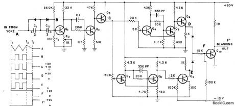
Prevents burning of phosphor on face of flying-spot stunner if sweep is lost. Consists of differentiator-amplifier, high and low-level detector, inverter, and summing and blanking generator. All transistors are 2N1302, and all diodes are 1N497.-Flying Spot Scanner Sweep Alarm, Electronic Circuit Design Handbook, Mactier Pub. Corp., N.Y., 1965, p 125. (View)
View full Circuit Diagram | Comments | Reading(684)
DUTY_CYCLE_CONTROL
Published:2009/7/1 20:17:00 Author:May
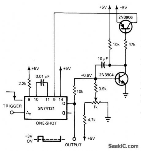
Feedback loop through two transistors automatically adjusts timing of MVBR to hold duty cycle constant over wide range of triggering rates. 2N3904 acts as integrator with time constant much longer than pulsing period. If duty cycle increases or decreases, current into integrator becomes positive or negative and DC voltage at its collector slowly decreases or increases. This collector voltage drives 2N3906 operating as current generator for adjusting automatically to give chosen duty cycle as selected by 1K pot. Range is 17% to above 50%.-J. L. Engle, Regulate Duty Cycle Automatically, EDN Magazine, Nov, 5, 1978, p 122. (View)
View full Circuit Diagram | Comments | Reading(855)
BICYCLE_SPEED_ALARM
Published:2009/7/1 19:50:00 Author:May

Useful for long-distance bicycling, to indicate when rider drops below predetermined minimum speed. Speed sensor is reed switch attached to frame and tripped once per revolution by permanent magnet mounted on wheel. Rate at which switch closes determines level of DC voltage produced by circuit. When voltage drops below preset level determined by 100K pot, output transistor comei on and energizes relay controlling bicycle hom or other signaling device. Supply can by 9-V transistor battery. Transistor reading should be high enough to handle relay used.-J. Sandler, 9 Projects under $9, Modem Electronics, Sept, 1978, p 35-39. (View)
View full Circuit Diagram | Comments | Reading(1176)
LED_BRIGHTNESS_CONTROL_1
Published:2009/7/1 5:38:00 Author:May
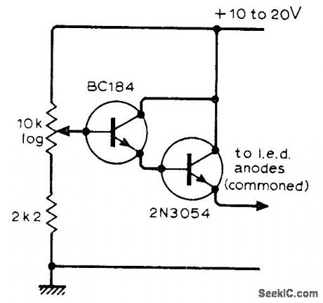
Uses 10K logarithmic pot to vary brightness simultaneously for all LEDs in digital display.-S.F.Bywatelsand J,E West,Peak-Reading Audio Level Indicator,Wireless World, Aug. 1975,p 357-36. (View)
View full Circuit Diagram | Comments | Reading(664)
VOLTAGE_CONTROLLED_MONO
Published:2009/7/1 4:52:00 Author:May

Timing period of opamp operating as monostable multivibrator is controlled by magnitude of DC reference voltage. With square-wave input shown. differentiating action by C1-R1 gives positive pulses that cause mono to make transitions. Article gives design equation and typical waveforms.-G. B. Clayton. Experiments with 0perational Amplifiers, Wireless World, May 1973, p241-242. (View)
View full Circuit Diagram | Comments | Reading(2770)
AUTOMATIC_BRIGHTNESS_CONTROL
Published:2009/7/1 4:44:00 Author:May

Circuit adjusts brightness of LED digital display by altering mark-space ratio of LED supply voltage.Ambient-light input is sensed by BC109C transistor with top taken off. Normal display current of 20 mA is reduced to 2 mA when darkened room makes brightness unnecessary, conserving battery life. Tr3 and Tr4 operate as Schmitt trigger, with mark time of 1.5 ms determined by R2 and space time controlled by charging current through Tr5 and Tr2 as affected by ambient light on Tr1. Article gives complete circuits for driving 11-LED array. To add brightness control circuit, break ground connection of LED supply transistors and insert saturated transistor Tr6.-G. Kalanit, Analogue to Digital Meter, Wireless World, July 1976, p 53-57.
(View)
View full Circuit Diagram | Comments | Reading(0)
PULSE_WIDTH_PROPORTIONAL_CONTROLLER_CIRCUIT
Published:2009/7/1 4:42:00 Author:May

The quad operational amplifier circuit yields full 0 to 100 percent pulse-width control.The controller uses an LM3900 that requires only a single supply voltage of 4 to 30 V.The pulse-repetition rate is set by a 1 kHz oscillator that incorporates amplifier A1. The oscillator feeds ramp generator A2, which generates a linear ramp voltage for each oscillator pulse. The ramp signal feeds the inverting input of comparator A3; the speed-control voltage feeds the noninverting input. Thus, the output of the comparator is a 1 kHz pulse train, the pulse width of which changes linearly with the control voltage.The control voltage can be provided by an adjustable potentiometer or by an external source of feedback information such as a motor-speed sensing circuit. Depending on the control-voltage setting, the pulse duration can be set at any value from zero (for zero average dc voltage applied to the motor) to the full pulse-repetition period (for applied motor voltage equal to dc power-supply voltage). An amplifier stage (A4) with a gain of 10 acts as a pulse-squaring circuit. A TIP-31 medium-power transistor is driven by A4 and serves as a separate power-amplifier stage. (View)
View full Circuit Diagram | Comments | Reading(1812)
SOLID_STATE_SWITCHING
Published:2009/7/24 4:02:00 Author:Jessie

Used in high-speed data transmission system having 15-gc bandwidth. Use of Kita diodes gives transition lime of 20 nsec for break and 40 nsec for restoration, pg compared to 1 millisec for reed relays.-I. Someya, Bidding For World Leadership in Solid State Micro. wave Gear, Electronics, 38:25, p 99-105. (View)
View full Circuit Diagram | Comments | Reading(629)
PUNCH_PRESS_SAFETY_SWITCH
Published:2009/7/24 4:02:00 Author:Jessie

Static switching control for dangerous presses requires that both hands of operator be on run push buttons, out of danger area, before ram can descend. To prevent operators from jamming or taping one or more buttons closed, control circuit stops press at end of cycle. Both buttons must then be released and depressed again to start new cycle. self-exched magnetic amplifier operates much like snap switch.-S. A. Zarleng, Static Switching Techniques for Machine-Tool Safety, Electronics, 32:24, p 57-59. (View)
View full Circuit Diagram | Comments | Reading(697)
MISSILE_COUNT_DOWN_SWITCH
Published:2009/7/24 4:01:00 Author:Jessie

Level-sensitive switch uses nonlinear negative feedback to provide stable operation (within 1.5%) over 100℃ temperature range. Monostable mvbr is followed by rectifying transistor and filter. For signals above trigger level, circuit is periodically switched into its transient stale.-D. W. Boensel, Switching Circuits for Missile Count-Downs, Electronics, 32;31, p 76-78. (View)
View full Circuit Diagram | Comments | Reading(517)
AUTOMATIC_LEVEL_CONTROL
Published:2009/7/1 4:31:00 Author:May

The NE570 can be used to make a very high performance ALC compressor, except that the rectifier input is tied to the input. This makes gain inversely proportional to input level so that a 20 dB drop in input level will produce a 20 dB increase in gain. The output will remain fixed at a constant level. As shown, the circuit wilt maintain an output level of ±1 dB for an input range of +14 to -43 dB at 1 kHz. Additional external components will allow the output level to be adjusted. (View)
View full Circuit Diagram | Comments | Reading(674)
OPERATIONAL_AMPLIFIER_CONTROL
Published:2009/7/24 3:55:00 Author:Jessie

Switch must pass 1 ma in either direction (A to B or B to A). Diode pairs D1-D2 and D3-D4 are voltage limiters, while Q1 is basic switching element. Switching time is about 2 microsec.Used as sample-and-hold circuit, with 500-microsec sampling interval-R. W. Maloy, Transistor Switch Passes Current Both Ways, Electronics, 38:1, p 79. (View)
View full Circuit Diagram | Comments | Reading(697)
AUDIO_AUTOMATIC_GAIN_CONTROL
Published:2009/7/1 4:24:00 Author:May

An audio signal applied to U1 is passed through to the 741 operational amplifier, U2. After being amplified, the output signal of U2 is sampled and applied to a negative voltage doubler/rectifier circuit composed of diodes CR1 and CR2 along with capacitor C1. The resulting negative voltage is used as a control voltage that is applied to the gate of the 2N5485 JFET Q1. Capacitor C2 and resistor R2 form a smoothing filter for the rectified audio control voltage.The JFET is connected from pin 2 of the MC3340P to ground through a 1 kilohm resistor. As the voltage applied to the gate of the JFET becomes more negative in, magnitude, the channel resistance of the JFET increases causing the JFET to operate as a voltage controlled resistor. The MC3340P audio attenuator is the heart of the AGC. It is capable of 13 dB gain or nearly -80 dB of attenuation depending on the external resistance placed between pin 2 and ground. An increase of resistance decreases the gain achieved through the MC3340P. The circuit gain is not entirely a linear function of the external resistance but approximates such behavior over a good portion of the gain/attenuation range. An input signal applied to the AGC input will cause the gate volt-age of the JFET to become proportionally negative. As a result the JFET increases the resistance from pin 2 to ground of the MC3340P causing a reduction in gain. In this way the AGC output is held at a nearly constant level. (View)
View full Circuit Diagram | Comments | Reading(1449)
| Pages:150/312 At 20141142143144145146147148149150151152153154155156157158159160Under 20 |
Circuit Categories
power supply circuit
Amplifier Circuit
Basic Circuit
LED and Light Circuit
Sensor Circuit
Signal Processing
Electrical Equipment Circuit
Control Circuit
Remote Control Circuit
A/D-D/A Converter Circuit
Audio Circuit
Measuring and Test Circuit
Communication Circuit
Computer-Related Circuit
555 Circuit
Automotive Circuit
Repairing Circuit