
Control Circuit
Index 156
DELAYED_ALARM
Published:2009/6/30 1:45:00 Author:May

When normally closed arm/disarm switch is opened, first section of NE556 dual timer starts its timing cyde. After delay to allow for entry or exit, pin 5 goes low to energize alarm circuit. Now as long as all door switches are dosed, PNP transistor is kept off because pin 9 is high. When any door switch is opened, transistor tums on after normal delay for owner to enter car, and hom is sounded unless owner closes arm/disarm switch within delay time.- Signetics Analog Data Manual, Signetics, Sunnyvale, CA, 1977, p 724-725. (View)
View full Circuit Diagram | Comments | Reading(0)
SILENT_ALARM
Published:2009/6/30 1:44:00 Author:May

When thief opens car door, relays K1 and K2 activate tone-modulated transmitter, which can be any legal combination of power, frequency, and antenna. A few milliwatts of power should be adequate. Thief hears nothing, but owner is alerted via portable receiver tuned to transmitter frequency. Transmitter remains on about 15 s (determined by R3 and C1) after door is closed until NE555 times out and removes power from transistor. Use any NPN transistor having adequatecurrent rating for relay. If alarm is provided with its own battery and whip antenna, it cannot be disabled from outside of car.-A. Day, Soundless Mobile Alarm, CQ, April 1977, p 11. (View)
View full Circuit Diagram | Comments | Reading(0)
CAR_THEFT_ALARM
Published:2009/6/30 1:42:00 Author:May

Alarm remains on even if signal from car door switch or other sensor is only momentary, so relay is wired to be selflatching until keyswitch S1 is tumed off. Use hood locks or hood-opening sensors to prevent thief from disabling alarm by cutting battery cable. Circuit indudes time delay of 6 s for entering car and shutting off alarm, to avoid need for extemal keyswitch. Sonalert makes loud tone during 6-s delay period to remind driver that alarm needs to be turned off. At end of 6 s, Sonalert stops and much louder bell is energized to further discourage intruder.-J. Pawlan, The Smart Alarm, 73 Magazind, June 1975. p 37-41. (View)
View full Circuit Diagram | Comments | Reading(861)
CASCODE_TONE_CONTROL
Published:2009/6/30 1:41:00 Author:May

Circuit raises 100-mV input signal level to 1V for driving power amplifier and uses cascode arrangement to im-prove S/N ratio of tone control network. Values show give maximum bass boost or cut at 50Hz with R19 and maximum treble boost or cut at 10kHz with R20,Tr2 can be BC15,BC214、BC309, or equivalent,Other transistors can be BC109、BC114、BC184, or equivalent.-J,N Ellis,Hiah Quality Tone Control, Wireless World Aug.1973、p378 (View)
View full Circuit Diagram | Comments | Reading(2062)
Switch_driver_with_micropower_standby_mode_18_V_to_28_V
Published:2009/7/24 20:56:00 Author:Jessie

Figure 8-54 shows an LTC1155 connected for switchldriver operation with micropower standby. This circuit is similar to that shown in Fig. 8-53, but with R1 increased from 3 kΩ to 330 kΩ, and a boot-strap R2/D2 network added. These modifications reduce the Fig. 8-54 standby current to less than 30 μA. The extra supply current is provided only when the switch is turned on. The supply current drops back to 30 μA when the switch is turned off, and the LTC1155 is returned to standby. LINEAR TECHNOLOGY, APPLICATION NOTE 53, P. 4, (View)
View full Circuit Diagram | Comments | Reading(508)
TWO_CHANNEL_PANNING
Published:2009/6/30 1:40:00 Author:May
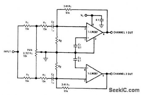
Provides smooth and accurate panoramic control of apparent microphone position between two output channels, as often required in mixing consoles at recording studios, Bequ ires only single linear pot. At each extreme of pot, gain is unity for one channel and zero for other. With pot centered, gains for both channels are -3 dB. R2 depends on supply voltage used, which can be from 9 to 30 V.- Audio Handbook, National Semicon-ductor, Santa Clara, CA, 1977, p 2-59-2-61. (View)
View full Circuit Diagram | Comments | Reading(722)
MALE_FEMALE_VOICE_SWITCH
Published:2009/6/30 1:39:00 Author:May

Circuit developed by NASA engineers to improve intelligibility of voice communication during Apollo moon shots passes only the three portions of the speech spectrum required for clear speech:300-400 Hz and 2500-3000 Hz for both sexes and 900-1700Hz for males or t 100-1900 Hz for females. Pot ad lusts null to about 600 Hz. Circuit improves readabilhy of weak DX voice signals in noise.-J. Fisk, Circuits and Techniques, Ham Radio, June 1976, p 48-52. (View)
View full Circuit Diagram | Comments | Reading(721)
WIDEBAND_AF_LEVEL_CONTROL
Published:2009/6/30 1:38:00 Author:May
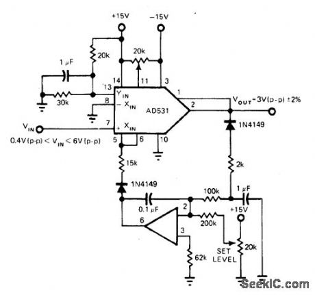
AD531 analog multipliercan hold outputto 3V P-P ±2% for inputs from 0.4 to 6V P-P、at frequencies from 30 Hz to 400 kHz Opamp type is not critical.-R Franlz, Analog Multipliers-New IC Versions Manipulate Real-World Phenomenawith Ease,EDN Magazine, Sept 5、1977,p 125-129. (View)
View full Circuit Diagram | Comments | Reading(520)
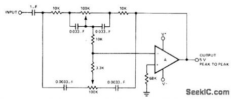
THUMPLESS_CONTROL
Published:2009/6/30 1:38:00 Author:May

Five-transistor circuit for audio amplifier applications eliminates thumping sounds that can sometimes be heard when Ievel of input signal changes suddenly.Differential amplifier Q1-Q2, with B, in emitter-current control circuit, eliminates thump. Control input acts on identical transistors Q3-Q4 which make transconductance of differential pair Q1-Q2 vary in direct proportion to control voltage. Fifth transistor in array, Q5, is used as outputsignal buffer. Amplifiergain is 30 for control voltage of 15 V.-P. Brokaw, Automatic Gain Control Quells Amplifier Thump, Electron-ics, Jan. 10, 1974, p 131-132; reprinted in Circuits for Electronics Engineers, Electronics, 1977, p 46-47. (View)
View full Circuit Diagram | Comments | Reading(689)
SOUND_OPERATED_RELAY
Published:2009/6/30 1:36:00 Author:May

Output of about 1.8 m VRMS from crystal orceramic microphone will energize relay when sensitivity control R4 is at maximum. First two stages form high-gain RC-coupled AF amplifier, output of which is rec-tified by silicon diode X1. DC voltage developed across diode is applied to gate of Siliconix U183 FETwhich acts as DC amplifier driving Sigma 5F or equivalent relay. To ad just, short microphone terminals, set R4 for maximum sensitivity, then ad just R10 until relay opens.-R. P Turner, FET Circuits, Howard W. Sams, Indianapolis, IN, 1977, 2nd Ed., p 111-113. (View)
View full Circuit Diagram | Comments | Reading(984)
ENTRY_DELAY_ALARM
Published:2009/6/30 1:35:00 Author:May

First 555 timer provides delay of about 20 s after triggering by sensor before alarm bell is energized, to allow thief to be caught inside house or give owner time to enter and shut off alarm. Alarm then rings for about 60 s under control of timer U2. Alarm period was set short to attract attention without unduly annoying neighbors.-J. D. Arnold, A Low-Cost Burglar Alarm for Home or Car, QST, June 1978, p 35-36. (View)
View full Circuit Diagram | Comments | Reading(813)
SCR_LATCH
Published:2009/6/30 1:34:00 Author:May

Turns on mobile transceiver or other mobile equipmentwhen powerisapplied, if external circuit is broken when equipment is stolen. Transmitter will then put unmodulated carrier on air even with PTT switch disconnected or off, for tracing with radio direction finder. If added components are carefully concealed in equipment and new external wiring is worked into existing wiring harness, few thieves will be able to locate trouble. External wires are run under dash so thief must cut them to get out equipment. PTT relay should have protective diode. SCR is 100 PIV, 1 A, but HEP R1003 or R1217 can also be used.-E. Noll, Circuits and Techniques, Ham Radio, April 1976, p 40-43. (View)
View full Circuit Diagram | Comments | Reading(1985)
FIVE_INDICATOR_ALARM
Published:2009/6/30 1:32:00 Author:May

Single five-transistor 10 uses NPN structures on P-type substrate as PNPN silicon controlled switches having common connection for anode (substrate).Relay serving as anode load is energized for actuating alarm if any of the SCS pushbutton switches is closed. Corresponding lamp is energized to identify door or window at which sensor switch has been closed by act of intruder. Alarm remains on until reset by interrupting power supply. Power drain on standby is negligible because SCSs act as open circuits until triggered, permtitting use of batteries for supply. Two or more ICs may be added to get more channels.-H. S. Kothari, Alarm System with Position Indication, Wireless World, Feb. 1976, p 77. (View)
View full Circuit Diagram | Comments | Reading(880)
4_μs_CONVERSION_TIME
Published:2009/6/29 23:58:00 Author:May

Provides conversion of analog input to 8-bit digital output by suc cessive approximation, with conversion time of 4 μs. Advanced Micro Devices AM2502 successive-approximation register contains logic for Precision Monolithics DAC-08E and CMP-01C comparator.—D. Soderquist and J. Schoeff, Low Cost, High Speed Analog-to-Digital Conversion with the DAC-08, Precision Monolithics, Santa Clara, CA, 1977, AN-16, p 3. (View)
View full Circuit Diagram | Comments | Reading(751)
TONE_CONTROL_FOR_OPAMP
Published:2009/6/29 23:55:00 Author:May
Provides up to 20 dB of bass boost or cut at 20 Hz and up to 19dB of treble boost or cut at 20 kHz. Turnover fre-quency is 1 kHz. Opamp can be 531 or 301.- Signetics Analog Data Manual, Sunnyvale, CA, 1977, p 638-640. (View)
View full Circuit Diagram | Comments | Reading(1758)
LOW_ON_LOGIC_CONTROL
Published:2009/6/29 23:53:00 Author:May
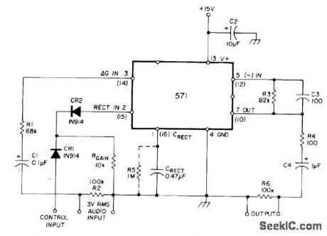
Uses Signetics NE571 or NE570 analog compandor. Gain is determined by current developed through RGAIN in conjunction with intemal 1.8-V voltage reference. When control input is low, normal current flowsthrough RGAIN When control signal is high, CR1 is forward-biased, interrupting current flow, and output is attenuated.-W. G. Jung, Gain Control IC for Audio Signal Processing, Ham Radio, July 1977, p 47-53. (View)
View full Circuit Diagram | Comments | Reading(865)
HIGH_ON_LOGIC_CONTROL
Published:2009/6/29 23:52:00 Author:May
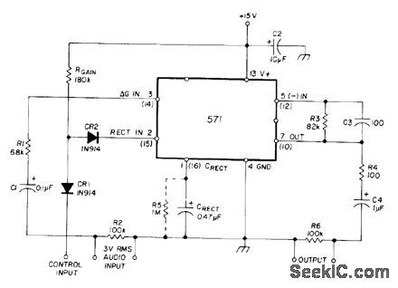
Uses Signetics NE571 or NE570 analog compandor. When control tnput is high, CR1 is off and current developed by RGAIN flows into rectifier input, allowing audio to be amplified. Gain is unity (or other nominal value chosen by changing value of R3) for control inputs greater than 3 V. Switching is abrupt, with full attenuation below 1.5 V. Narrow transition width and nominal DC center of 1.8 V allow direct control from CMOS, rrL, DTL, or other positive logic. Supply voltage should be stable.-W. G. Jung, Gqin Control IC for Audio Signal Processing, Ham Radio, July 1977, p47-53. (View)
View full Circuit Diagram | Comments | Reading(940)
BASS_TREBLE_BOOST_CUT
Published:2009/6/29 23:52:00 Author:May
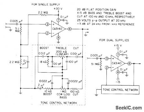
Using linear and log pots with tone control network in feedback path of CA3140 bipolar MOS opamp, circuit provides 20-dB gain in flat position and ±15dB bass and treble boost and cut at 100 and 10,000 Hz.Output is 25 V P-P at 20 kHz and is -3 dB at 24 kHz from 1-kHz reference. Optional connection for ±15V supply is also shown.- Circuit Ideas for RCA Linear ICs, RCA Solid State Division, Somerville, NJ, 1977, p 10. (View)
View full Circuit Diagram | Comments | Reading(2060)
CONSTANT_18_V_AF_FOR_SSB
Published:2009/6/29 23:50:00 Author:May
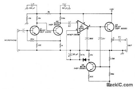
Uses Motorola MFC6040 voltage-controlled amplifierIC having 13-dB gain.and maximum of 90-dB gain reduction. Q1-Q2 form microphone preamp, Q4 is AGC detector/amplifier for IC, and a3 is output buffer. With 500-ohm dynamic microphone, output remains constant at 1.8 VRMS.-L. No-votny, Speech Compressor, Ham Radio, Feb.1976, p 70-71. (View)
View full Circuit Diagram | Comments | Reading(2318)
ROOM_E0UALIZER
Published:2009/6/29 23:48:00 Author:May
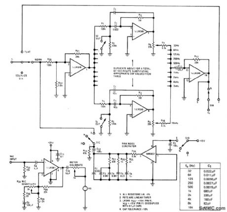
Ten-octave equalizer is combined with pink-noise generator in such away that all but one octave band can be switiched out,Mith pink noise passed through remaining filter to power amplifier and loudspeaker,Microphone with flat frequency response over audio band is used to pick up resulting noise at some center listening point in room being equalized. Ampllfied output ot microphone drives VU meter where arbitrary level is established for one filter section. Other filter sections are then switched in one at a time and adjusted to give same VU reading. Equalizer settings then give flat room response for all ten octaves. High end can then be rolled off or low end boosted to suit personal preference. Adjustments are readily repeated when fumiture is changed in room. Table gives values of C1 for each octave.- Audio Handbook, National Semiconductor, Santa Clara, CA, 1977, p 2-53.-2-59. (View)
View full Circuit Diagram | Comments | Reading(1001)
| Pages:156/312 At 20141142143144145146147148149150151152153154155156157158159160Under 20 |
Circuit Categories
power supply circuit
Amplifier Circuit
Basic Circuit
LED and Light Circuit
Sensor Circuit
Signal Processing
Electrical Equipment Circuit
Control Circuit
Remote Control Circuit
A/D-D/A Converter Circuit
Audio Circuit
Measuring and Test Circuit
Communication Circuit
Computer-Related Circuit
555 Circuit
Automotive Circuit
Repairing Circuit