
Time Control
Index 4
SIMPLE_TIMER
Published:2009/6/29 2:33:00 Author:May

Press S1. The 100 μF electrolytic capacitor rapidly charges up at about 0.7 V. The transistor will be forward biased, and collector current will flow operating the relay. Release S1. The capacitor will begin to discharge via the 33 K resistor at the base of the transistor. When the voltage across the capacitor gets down to half a volt or so, the transistor base will no longer be forward biased, collector current will cease, and the relay will drop out. The capacitor will continue to discharge via the 47 K resistor. With the values shown, the relay will remain operated for about eight seconds. Long times are possible with lower values of capacitance by substituting a Darlington pair for the 2N2926. In this case, increase the two resitor values into the megohm range. (View)
View full Circuit Diagram | Comments | Reading(863)
TIMING_CIRCUIT
Published:2009/6/29 2:31:00 Author:May

Load current starts approximately 0.5 RC after the switch IS thrown. (View)
View full Circuit Diagram | Comments | Reading(0)
ELECTRONIC_EGG_TIMER
Published:2009/6/29 2:29:00 Author:May

The IC functions as an af multivibrator which is controlled by the external transistor. S1A/B is the on-off toggle switch. (View)
View full Circuit Diagram | Comments | Reading(1043)
PRECISION_SOLID_STATE_TIME_DELAY_CIRCUIT
Published:2009/6/29 2:28:00 Author:May

Time delays from 0.3 milliseconds to over three minutes are possible with this circuit without using a tantalum or electrolytic capacitor. The timing interval is initiated by applying power to the circuit. At the end of the timing interval, which is determined by the value of R1C1, the 2N494C fires the controlled rectifier. This places the supply voltage minus about one volt across the load. Load currents are limited only by the rating of the controlled rectifier which is from 1 ampere up to 25 am-peres for the types specified in the circuit. A calibrated potentiometer could be used in place of R1 to permit setting a predetermined time delay after one initial calibration. (View)
View full Circuit Diagram | Comments | Reading(826)
SOLID_STATE_TIMER_FOR_INDUSTRIAL_APPLICATIONS
Published:2009/6/29 2:27:00 Author:May


View full Circuit Diagram | Comments | Reading(934)
TIME_DELAYED_RELAY_FOR_PATIO_LIGHT,GARAGE_LIGHT,ENLARGER_PHOTOTIMER,ETC
Published:2009/6/29 2:24:00 Author:May

This simple timing circuit cat: delay an output switching function from.01 seconds to about 1 minute. The SCR is triggered by only a few microamps from the timing network R1-C1 to energize the output relay. (View)
View full Circuit Diagram | Comments | Reading(664)
DARKROOM_TIMER
Published:2009/6/24 23:13:00 Author:May

The electronic darkroom timer is built around a 555 oscillator/timer, a pair of general-purpose transistors, a buzzer, and an LED. The 555 (U1) is configured as an astable multivibrator (free-rututing oscillator). The frequency of the oscillator is determined by the values R1 through R3 and C1 through C4.
Switch S1 is used to divide the capacitor network to vary the time interval between beeps; when S1 is closed, the circuit beeps at intervals of 30 seconds. With S1 closed, it beeps at 15-second intervals.
When power is applied to the circuit (by closing switch S2), the output of U1 at pin 3 is initially high. That high is applied to the base of transistor Q1 (an MPS2907 general-purpose pnp device), keeping it turned off. That high is also applied to the anode of LED1 (which is used as a power on indicator) through resistor R7, turning it on.
Timing capacitors C1 through C5 begin to charge through timing resistors R1 through R3. dc voltage is applied to BZ1's driver input through R5 and to its feedback terminal (through R4), which is also connected to Q2's base terminal. The V+ voltage that applied to Q2's base causes it to turn on, tying BZ1's common terminal high.
When the timing capacitors are sufficiently charged, a trigger pulse is applied to pin 2 (the trigger input) of U2, causing U1's output to momentarily go low. This causes LED1 to go out and tran-sistor Q1 to turn on. That, in turn, grounds the common lead of buzzer BZ1, causing BZ1 to sound. Afterward, the output of U1 returns to the high state, turning off Q1, and turning on LED1, until another time interval has elapsed and the process is repeated.
The circuit is powered by a 9-Vac adapter, which plugs into a standard 117-V household outlet. Because the circuit draws only about 10 to 15 mA, a 9-V alkaline transistor-radio-battery can also be used to power the circuit. (View)
View full Circuit Diagram | Comments | Reading(0)
TREBLE_CONTROL_CIRCUIT
Published:2009/6/24 4:40:00 Author:May

This tone control has an insertion loss of 20 dB at flat setting and is effective above 1 kHz,It little effect below about 1 kHz. (View)
View full Circuit Diagram | Comments | Reading(0)
LOW_FREQUENCY_CLOCK
Published:2009/6/22 22:50:00 Author:May

The LM3090 is an LED flasher IC that is designed to oscillate at low frequencies. The clock out-put of the first circuit can be changed by changing the value of the capacitor, and the second circuit lets you adjust the frequency with the trimmer. BI can be one or two alkaline 1.5-V cells. The LM3909 can supply up to 45-mA pulses at greater than 2V. (View)
View full Circuit Diagram | Comments | Reading(899)
SELF_RETRIGGERING_TIMED_ON_GENERATOR
Published:2009/6/22 22:47:00 Author:May
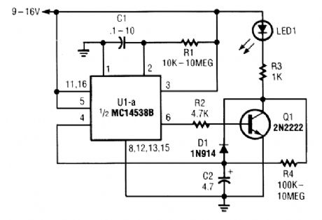
When power is first applied to the circuit, CZ begins to charge via LED1, R3, and R4. When the voltage across C2 reaches UI's input trigger level, the output of UI at pin 6 goes positive for a period that is determined by the values of C1 and R1. That turns Q1 on, discharging C2 through Dl and Q1.
At the end of the set period, the output of UI at pin 6 goes low, turning Q1 off and allowing the current to begin flowing through LED1, R3, and R4 to gain charge C2, causing the cycle to repeat.The repeat time is determined by the values of R3, R4, and C2. The previous formula won't be as accurate for this circuit, but it will at least get you close enough for the capacitor value; then R4, can be fine-tuned to obtain the desired timing period. (View)
View full Circuit Diagram | Comments | Reading(0)
LONG_DELAY_PERIOD_TIMER
Published:2009/6/18 3:37:00 Author:May

This method of obtaining a 4 to 40 hour timing period from a 555 IC can be further expanded to produce even longer delays with equal accuracy. (View)
View full Circuit Diagram | Comments | Reading(1231)
VCR_VIDEO_DETECTOR_CONTROLLER
Published:2009/6/18 3:36:00 Author:May

This circuit uses the video output from a VCR or camera to control a relay. Video turns on Q1, cutting off Q2, allowing Q3 to be forward biased, activating relay K1. You can use the timer in your VCR and this unit to generate long time delays as well. (View)
View full Circuit Diagram | Comments | Reading(1452)
THREE_STAGE_SEQUENTIAL_TIMER_
Published:2009/6/18 3:14:00 Author:May

By using three 555 ICs, three sequential pulses can be generated. Output 3 can be connected back to trigger input to achieve astable operation. (View)
View full Circuit Diagram | Comments | Reading(1455)
TELE_TIMER
Published:2009/6/18 3:11:00 Author:May

The circuit is built around a 555 oscillator/ timer. The circuit provides two time periods. The long-running time period is adjustable from about 1 to 10 minutes, and the short time period is pre-set to about three seconds.
Here's how the dual timer operates. When the power is switched on, C2 begins to charge through R3, R1, Dl, and R4 to start the long-term timer period. When the voltage across C2 reaches the 555's internal switching point, the long-term timer times out, discharging C2 throughR2, D2, and pin7 ofthe 555. Duringthat time, pin 3 of the 555 is pulled to ground, acti-vating the piezo sounder.To set the short time period to about four seconds, use a 10 k resistor for R2, and for about twenty seconds use a 47 k resistor. The timing capacitor, C2, should be a good-quality, low-leakage unit. (View)
View full Circuit Diagram | Comments | Reading(920)
SIMPLE_TIME_DELAY_CIRCUIT
Published:2009/6/18 3:02:00 Author:May

Rotating the potentiometer wiper will change the time delay from the 555 IC. (View)
View full Circuit Diagram | Comments | Reading(963)
ELECTRONICS_NOW
Published:2009/6/18 2:59:00 Author:May


This timer circuit uses a 555IC timer and three 74LS193 counters to drive an LED display. S1 is activated by one person, who tums on piezo buzzer BZ1 via Q1 and also starts the clock; S1 is acti-vated by the other person being timed. This shuts off the timer, and the number of LEDs lit indicate, in binary form, the elapsed time. (View)
View full Circuit Diagram | Comments | Reading(2029)
WATCH_TICK_TIMER
Published:2009/6/17 3:56:00 Author:May

This circuit adapts a frequency counter to measure intervals. It was originally used as a shutter speed checker for a photo ap-plication. The watch ticks are clipped and shaped and formed into a square wave. This square wave is used to gate an accurately known clock (1-MHz TTL XTAL OSC) and an external counter is used to directly count the clock pulses during the interval to be measured. A 1-MHz clock can be used to measure to a resolution of 1 psec. Accuracy = ± time base ±1 μs ±t1 count LSB. (View)
View full Circuit Diagram | Comments | Reading(766)
POWER_ON_DELAY_CIRCUIT
Published:2009/6/15 22:06:00 Author:May

Using an IC to count ac mains pulses, the circuit produces 16 various delay times,where ac power is applied to a load after a preset interval. (View)
View full Circuit Diagram | Comments | Reading(2185)
Timing controller circuit diagram 3
Published:2011/7/26 2:04:00 Author:Ecco | Keyword: Timing controller

The timing controller circuit is composed of the power supply circuit and timing control circuit, and it is shown as the chart. Power supply circuit is composed of the power control button S1, normally open contact K1 of relay K, buck capacitor C1, discharge resistor R1, rectifier diodes VD1 ~ VD4, filter capacitor C2 and zener diode VS. Timing control circuit is composed of the time-base integrated circuit IC, delaying time selection switch S2, resistors R2 ~ R5, capacitors C3, C4, light-emitting diode VL, relay K and diode VD5.
(View)
View full Circuit Diagram | Comments | Reading(692)
Timing controller circuit diagram 4
Published:2011/7/26 2:08:00 Author:Ecco | Keyword: Timing controller

The timing controller circuit is composed of the power supply circuit, input control circuit, timing circuit and output control circuit, and it is shown as the chart. The power supply circuit is composed of the step-down capacitor C6, discharge resistor R6, bridge rectifier UR, filtering capacitors C5, C4 and the voltage regulator diode VS. The input control circuit is composed of the piezoelectric ceramic BC on electronic alarm clock, capacitor C1, resistors RI, transistor VI. Timing circuit consists of resistors R1 ~ R5, reset button S1, regular timing switch S2, capacitors C2 and C3, light-emitting diode VL, time-based integrated circuit IC.
(View)
View full Circuit Diagram | Comments | Reading(616)
| Pages:4/6 123456 |
Circuit Categories
power supply circuit
Amplifier Circuit
Basic Circuit
LED and Light Circuit
Sensor Circuit
Signal Processing
Electrical Equipment Circuit
Control Circuit
Remote Control Circuit
A/D-D/A Converter Circuit
Audio Circuit
Measuring and Test Circuit
Communication Circuit
Computer-Related Circuit
555 Circuit
Automotive Circuit
Repairing Circuit