Index 25
ICL8023 three programmable op amp and its pin main characteristics
Published:2013/1/5 23:58:00 Author:Ecco | Keyword: three, programmable op amp , pin main characteristics
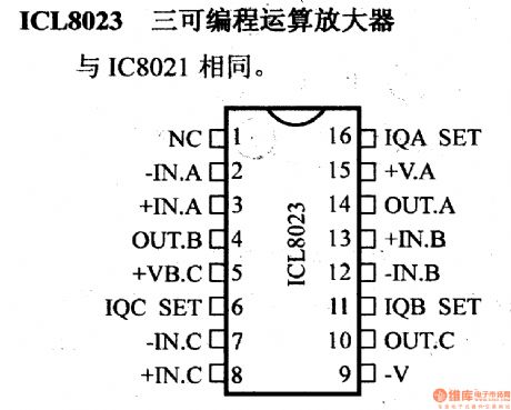
It is same with IC8021.
(View)
View full Circuit Diagram | Comments | Reading(707)
LF353 dual JFET input op amp and its pin main characteristics
Published:2013/1/6 0:20:00 Author:Ecco | Keyword: dual JFET, input op amp , pin main characteristics
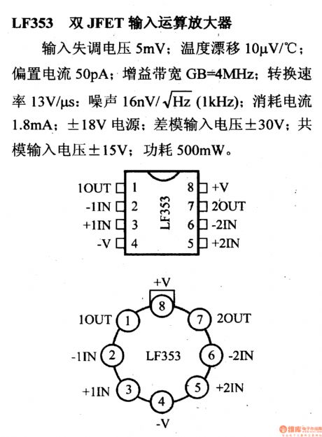
5mV input offset voltage; 10 μV / ℃ temperature drift; 50pA bias current; gain bandwidth GB = 4MHz; 13V/μs conversion rate; 1.8mA Current consumption; ± 18V power supply; ± 30V differential-mode input voltage; ± 15V common-mode input voltage; 500mW power consumption.
(View)
View full Circuit Diagram | Comments | Reading(2354)
MAX4108/MAX4109 high - speed operational amplifier and its pin main characteristics
Published:2013/1/6 0:32:00 Author:Ecco | Keyword: high - speed operational amplifier , pin main characteristics
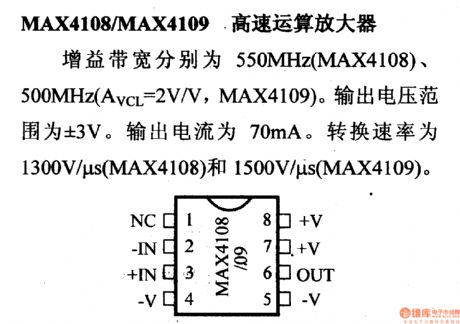
Gain bandwidth is 550MHz ( MAX4108 ), 500MHz ( AVCL and = 2V / V , MAX4109 ). Output voltage range is ± 3V. The output current is 70mA. Conversion rate is 1300V/μs (MAX4108) and 1500V/μs ( MAX4109 ).
(View)
View full Circuit Diagram | Comments | Reading(579)
MAX473/MAX474 single supply dual operational amplifier and its pin main characteristics
Published:2013/1/6 0:40:00 Author:Ecco | Keyword: single supply , dual operational amplifier , pin main characteristics
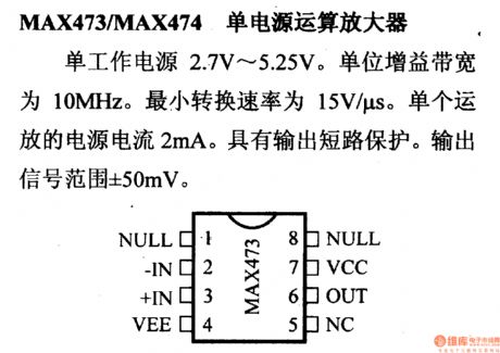
Single power supply is 2.7~5.25V. Unity-gain bandwidth is 10MHz. The minimum conversion rate is 15V/μ s. A single amplifier supply current is 2mA. It has output short circuit protection function. Output signal range is ± 50mV.
(View)
View full Circuit Diagram | Comments | Reading(636)
MAX494 quad operational amplifier and its pin main characteristics
Published:2013/1/6 0:27:00 Author:Ecco | Keyword: quad operational amplifier , pin main characteristics
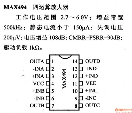
Operating voltage range is 2.7 to 6.0V; Gain Bandwidth is 500kHz; quiescent current is less than 150μA; offset voltage is 200μV; voltage gain is 108dB ; CMRR = PSRR = 90dB; driving load is 1kΩ.
(View)
View full Circuit Diagram | Comments | Reading(690)
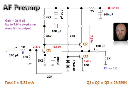
Boot-strapped Popcorn AF Feedback Pair
Published:2013/1/5 21:24:00 Author:muriel | Keyword: Boot-strapped, Popcorn AF, Feedback Pair
View full Circuit Diagram | Comments | Reading(761)
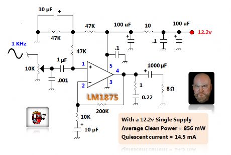
LM1875 Audio Power Amplifier
Published:2013/1/5 21:16:00 Author:muriel | Keyword: LM1875 , Audio, Power Amplifier
View full Circuit Diagram | Comments | Reading(2725)
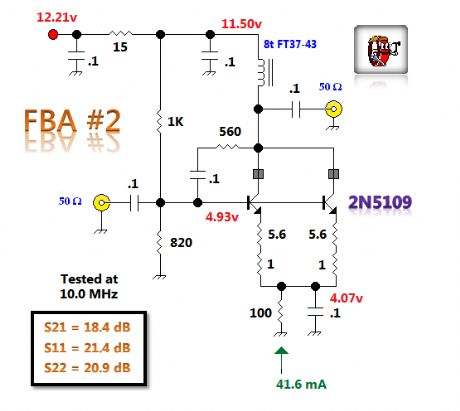
Parallel Transistor Feedback Amp
Published:2013/1/5 20:52:00 Author:muriel | Keyword: Parallel Transistor, Feedback Amp
View full Circuit Diagram | Comments | Reading(932)
Feedback Amplifier 2
Published:2013/1/5 20:51:00 Author:muriel | Keyword: Feedback Amplifier
View full Circuit Diagram | Comments | Reading(631)
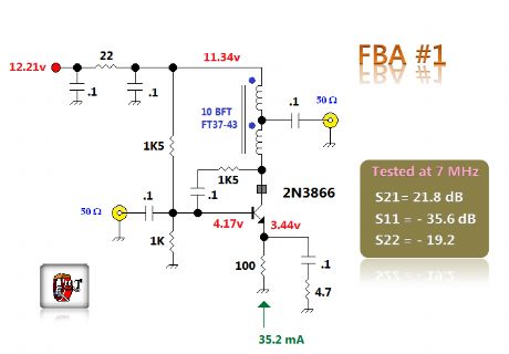
Feedback Amplifier 1
Published:2013/1/5 20:50:00 Author:muriel | Keyword: Feedback Amplifier
View full Circuit Diagram | Comments | Reading(549)
LM392 comparison amplifier and its pin main characteristics
Published:2013/1/5 1:06:00 Author:Ecco | Keyword: comparison amplifier , pin main characteristics
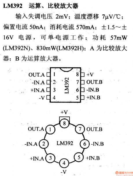
2mV input offset voltage; 7μV / ℃ temperature drift; 50nA bias current; 570mA current consumption; ± 1.5 to ± 16V power supply, and it can be a single power supply; 57mW ( LM392N ) power consumption, 830mW ( LM392H ) power consumption; A is a comparison amplifier; B is the operational amplifier.
(View)
View full Circuit Diagram | Comments | Reading(1329)
LM4250 low-power programmable amplifier and its pin main characteristics
Published:2013/1/5 1:27:00 Author:Ecco | Keyword: low-power, programmable amplifier, pin main characteristics
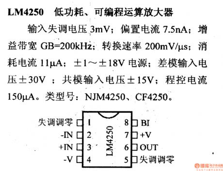
3mV Input offset voltage; 7.5nA bias current; gain bandwidth GB = 200kHz; 200mV/μs conversion rate; 11μA current consumption; ± 1 to ± 18V power supply; ± 30V differential-mode input voltage; ± 15V common-mode input voltage; 150μA programmable current. Type number: NJM4250.CF4250.
(View)
View full Circuit Diagram | Comments | Reading(766)
LM6161/6261/6361 operational amplifier and its pin main characteristics
Published:2013/1/5 1:19:00 Author:Ecco | Keyword: operational amplifier , pin main characteristics
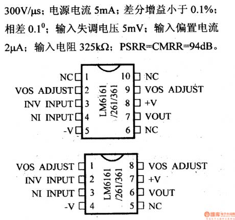
4.75 to 32V operating voltage range; 300V/μs conversion rate; 5mA supply current; differential gain is less than 0.1%; difference is less than 0.1 °; input offset voltage is 5mV; input bias current is 2μA; PSRR = CMRR = 94dB; input resistance is 325Ω.
(View)
View full Circuit Diagram | Comments | Reading(711)
LM6164/6264/6364 operational amplifier and its pin main characteristics
Published:2013/1/5 1:13:00 Author:Ecco | Keyword: operational amplifier, pin main characteristics
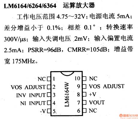

4.75 to 32V operating voltage range; 300V/μs conversion rate; 725MHz gain bandwidth; 5mA supply current; differential gain is less than 0.1%; difference is less than 0.1 °; input offset voltage is 2mV; input bias current is 2.5mA; PSRR = 96dB CMRR = 105dB; Gain Bandwidth Product GB = 175MHz.
(View)
View full Circuit Diagram | Comments | Reading(674)
LM6165/6265/6365 operational amplifier and its pin main characteristics
Published:2013/1/5 1:11:00 Author:Ecco | Keyword: operational amplifier , pin main characteristics
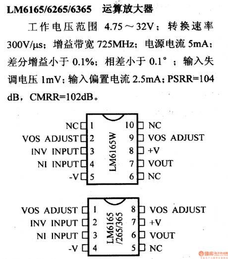
4.75 to 32V operating voltage range; 300V/μs conversion rate; 725MHz gain bandwidth; 5mA supply current; differential gain is less than 0.1%; difference is less than 0.1 °; input offset voltage is 1mV; input bias current is 2.5mA; PSRR = 104dB CMRR = 1.2dB.
(View)
View full Circuit Diagram | Comments | Reading(608)
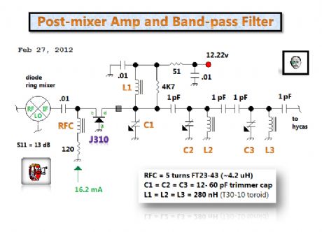
post-mixer amp
Published:2013/1/4 20:46:00 Author:muriel | Keyword: post-mixer amp
View full Circuit Diagram | Comments | Reading(1149)
ICL7641/7642 four CMOS operational amplifier and its pin main characteristics
Published:2013/1/4 2:07:00 Author:Ecco | Keyword: four CMOS , operational amplifier , pin main characteristics
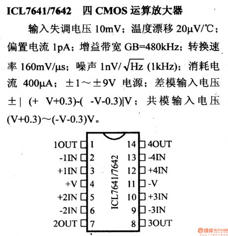
10mV Input offset voltage; 20μV / ℃ temperature drift; 1pA bias current; Gain Bandwidth GB = 480kHz; conversion rate 160mV/μs; 1nV / √ ˉ Hz ( 1kHz) noise; 400μA Current consumption; ± 1 to ± 9V power supply; ( V +0.30 ~~ ( - v- 0.3) V Total mode input voltage.
(View)
View full Circuit Diagram | Comments | Reading(683)
ICL8007 / A JFET input op amp and its pin main characteristics
Published:2013/1/4 2:13:00 Author:Ecco | Keyword: JFET input op amp , pin main characteristics
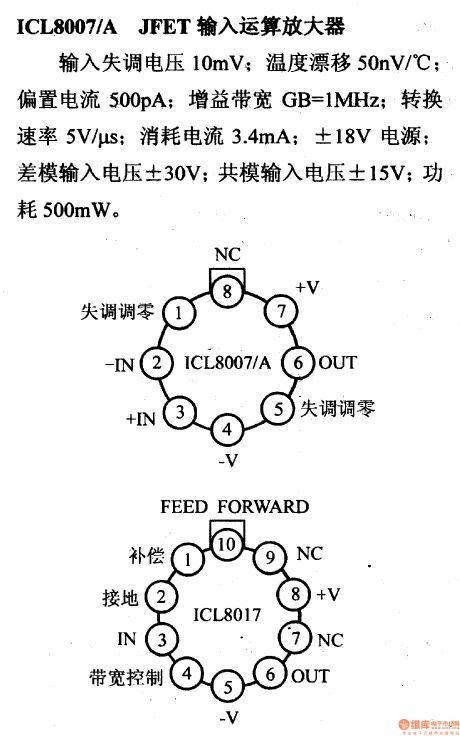
10mV Input offset voltage; 50μV / ℃ temperature drift; 500pA bias current; Gain Bandwidth GB = 1MHz; 5V/μs conversion rate; 3.4mA Current consumption; ± 18V power supply; ± 30V differential-mode input voltage; ± 15V common-mode input voltage; 500mW power.
(View)
View full Circuit Diagram | Comments | Reading(732)
ICL8021 programmable operational amplifier and its pin main characteristics
Published:2013/1/4 2:18:00 Author:Ecco | Keyword: programmable operational amplifier, pin main characteristics
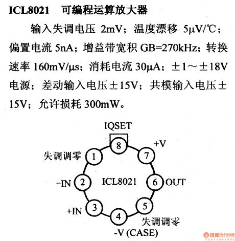
2mV Input offset voltage; 5μV /℃ temperature drift; 5nA bias current; Gain Bandwidth GB = 370kHz; 160mV/μs conversion rate; 30μA current consumption; ± 1 to ± 18V power supply; ± 15V differential-mode input voltage; ± 15V common-mode input voltage; 300mW allows loss.
(View)
View full Circuit Diagram | Comments | Reading(640)
ICL8022 dual programmable op amp and its main pin characteristics
Published:2013/1/4 1:20:00 Author:Ecco | Keyword: dual , programmable op amp, main pin characteristics
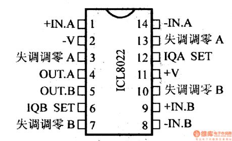
It is same with ICL8021.
(View)
View full Circuit Diagram | Comments | Reading(563)
| Pages:25/250 At 202122232425262728293031323334353637383940Under 20 |
Circuit Categories
power supply circuit
Amplifier Circuit
Basic Circuit
LED and Light Circuit
Sensor Circuit
Signal Processing
Electrical Equipment Circuit
Control Circuit
Remote Control Circuit
A/D-D/A Converter Circuit
Audio Circuit
Measuring and Test Circuit
Communication Circuit
Computer-Related Circuit
555 Circuit
Automotive Circuit
Repairing Circuit
