Index 153
METER_AMPLIFIER_FOR_15_V_SUPPLY
Published:2009/6/24 22:04:00 Author:May
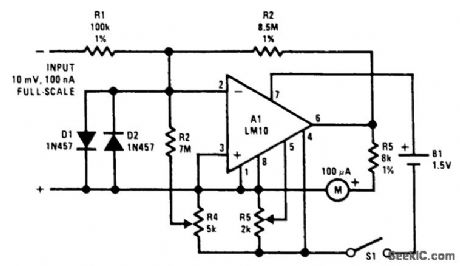
Art LM10 is used as a meter amplifier. Accuracy can be maintained over a 15℃ to 55℃ range for a full-scale sensitivity of 10 mV and 100 nA. The offset voltage error is nulled with R5, and the bias current can be balanced out with R4. The zeroing circuits operate from the reference output and are essentially unaffected by changes in battery voltage, so frequent adjustments should not be neces-sary. Total current drain is under 0.5 mA, giving an approximate life of 3 to 6 months with an AA cell and over a year with a D cell. With these lifetimes, an ON/OFF switch might be unnecessary. A test switch that converts to a battery-test mode might be of greater value. (View)
View full Circuit Diagram | Comments | Reading(582)
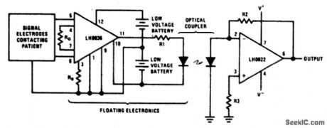
ISOLATION_AMPLIFIER_FOR_MEDICAL_TELEMETRY
Published:2009/6/24 22:02:00 Author:May
View full Circuit Diagram | Comments | Reading(514)
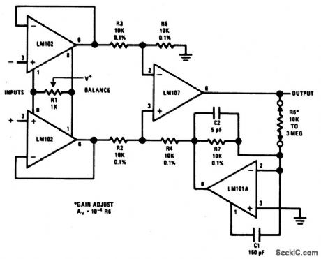
2INSTRUMENTATION_AMPLIFIER
Published:2009/6/24 22:02:00 Author:May

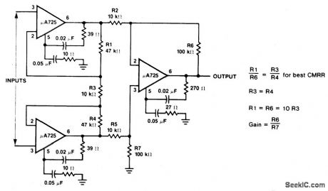
Three-amplifier circuit consumes only 135μW of power from a ±1.5 V power supply.With a gain of 101, the instrumentation amplifier is ideal in sensor interface and biomedical preamplifier applications. The first stage provides all of the gain while the second stage is used to provide common mode rejection and double-ended to single-ended conversion. (View)
View full Circuit Diagram | Comments | Reading(0)
OSCILLOSCOPE_PREAMPLIFIER
Published:2009/6/24 21:59:00 Author:May
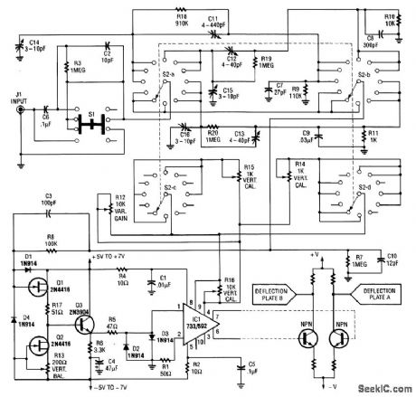
An oscilloscope front-end amplifier can be built with low-cost transistor and video amp ICs. This preamp uses a FET input and compensated attenuators, and has approximately 100-MHz bandwidth, which is adequate for most general-purpose oscilloscopes. (View)
View full Circuit Diagram | Comments | Reading(3523)
VOLTAGE_CONTROLLED_AUDIO_AMPLIFIER
Published:2009/6/24 21:56:00 Author:May
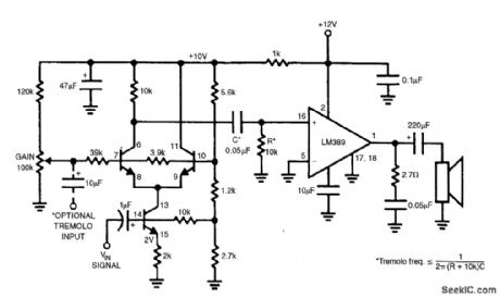
The LM389 has internal transistors used in this circuit. (View)
View full Circuit Diagram | Comments | Reading(1347)
VOLTAGE_CONTROLLED_AMPLIFIER
Published:2009/6/24 21:55:00 Author:May
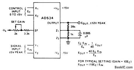
A constant or varying signal applied to the X input, Ec, controls the gain for a constant or vari-able signal applied to the Y input, Ein. The inputs could be interchanged.For this circuit, the set gain potentiometer is typically adjusted to provide a calibration for gain of Z 10 per-V-of-Ec. The bandwidth is dc to 30 kHz, independent of the gain. The wideband noise (10 Hz to 30 kHz) is 3 mV rms, typically, corresponding to full-scale signal-to-noise of 70 dB. Noise, referred to the signal input (Ec=±5V) is 60μV rms, typically. (View)
View full Circuit Diagram | Comments | Reading(0)
VIDEO_LINE_DRIVER
Published:2009/6/24 21:53:00 Author:May
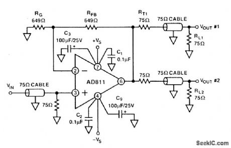
This video buffer/line driver operates at a gain of +2 and drives a pair of 75-Ω lines with 75-Ω back terminations. The overall terminated gain is unity. (View)
View full Circuit Diagram | Comments | Reading(746)
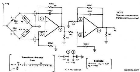
BRIDGE_TRANSDUCER_AMPLIFIER
Published:2009/6/24 21:52:00 Author:May
View full Circuit Diagram | Comments | Reading(1029)
VIDEO_DRIVER_AMPLIFIER
Published:2009/6/24 21:52:00 Author:May
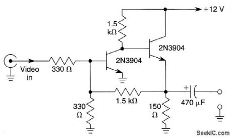
This simple circuit has a voltage gain of about 5x and will drive low-impedance loads (75 Ω) to 1.5 V p-p or better. (View)
View full Circuit Diagram | Comments | Reading(693)
250_mA_60_MHz_CURRENT_FEEDBACK_AMPLIFIER_FOR_VIDEO_APPLICATIONS
Published:2009/6/24 21:51:00 Author:May
View full Circuit Diagram | Comments | Reading(452)
BATTERY_POWERED_BUFFER_AMPLIFIER_FOR_STANDARD_CELL
Published:2009/6/24 21:51:00 Author:May

This circuit has negligible loading and disconnects the cell for low supply voltage or overload on output. The indicator diode extinguishes as disconnect circuitry is activated. (View)
View full Circuit Diagram | Comments | Reading(507)
CHOPPER_CHANNEL_AMPLIFIER
Published:2009/6/24 21:50:00 Author:May
View full Circuit Diagram | Comments | Reading(444)
VIDEO_AMPLIFIER
Published:2009/6/24 21:50:00 Author:May
View full Circuit Diagram | Comments | Reading(0)
VIDEO_SUMMING_AMPLIFIER
Published:2009/6/24 21:50:00 Author:May
View full Circuit Diagram | Comments | Reading(472)
LOW_SIGNAL_LEVEL,HIGH_IMPEDANCE_INSTRUMENTATION_AMPLIFIER
Published:2009/6/24 21:49:00 Author:May
View full Circuit Diagram | Comments | Reading(711)
1INSTRUMENTATION_AMPLIFIER
Published:2009/6/24 21:48:00 Author:May
View full Circuit Diagram | Comments | Reading(0)
VARIABLE_GAIN,DIFFERENTIAL_INPUT_INSTRUMENTATION_AMPLIFIER
Published:2009/6/24 21:48:00 Author:May
View full Circuit Diagram | Comments | Reading(500)
LEVEL_SHIFTING_ISOLATION_AMPLIFIER
Published:2009/6/24 21:47:00 Author:May
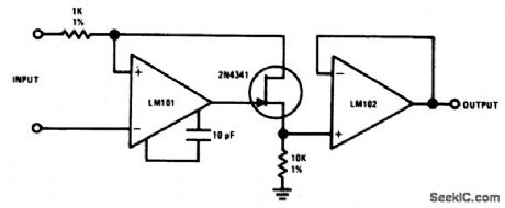
The 2N4341 JFET is used as a level shifter between two op amps operated at different power supply voltages. The JFET is ideally suited for this type of application because ID=IS. (View)
View full Circuit Diagram | Comments | Reading(829)
LM12O1_VIDEO_AMPLIFIER
Published:2009/6/24 21:46:00 Author:May
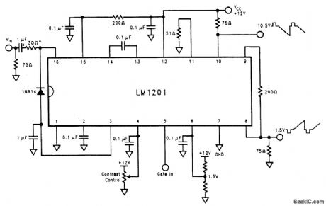
This video amplifier has 75-Ω bi-phase outputs. (View)
View full Circuit Diagram | Comments | Reading(479)
INSTRUMENTATION_AMPLIFIER_WITH_HIGH_COMMON_MODE_REJECTION
Published:2009/6/24 21:46:00 Author:May
View full Circuit Diagram | Comments | Reading(588)
| Pages:153/250 At 20141142143144145146147148149150151152153154155156157158159160Under 20 |
Circuit Categories
power supply circuit
Amplifier Circuit
Basic Circuit
LED and Light Circuit
Sensor Circuit
Signal Processing
Electrical Equipment Circuit
Control Circuit
Remote Control Circuit
A/D-D/A Converter Circuit
Audio Circuit
Measuring and Test Circuit
Communication Circuit
Computer-Related Circuit
555 Circuit
Automotive Circuit
Repairing Circuit
