Index 22
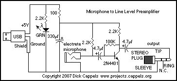
Electrete Condenser Microphone Line Level Preamp Project
Published:2013/1/22 21:16:00 Author:muriel | Keyword: Electrete Condenser , Microphone, Line Level , Preamp
View full Circuit Diagram | Comments | Reading(2761)
MC1420/1520 wideband op amp and its pin main characteristics
Published:2013/1/22 1:32:00 Author:Ecco | Keyword: wideband op amp , pin main characteristics
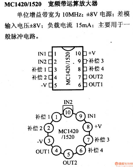
The unity-gain bandwidth is 10MHz; differential-mode input voltage is ± 8V; load current is 15mA; it is mainly used for general pulse circuit.
(View)
View full Circuit Diagram | Comments | Reading(824)
MC14573 quad CMOS programmable operational amplifier and its pin main characteristics
Published:2013/1/22 1:55:00 Author:Ecco | Keyword: quad CMOS, programmable, operational amplifier, pin main characteristics
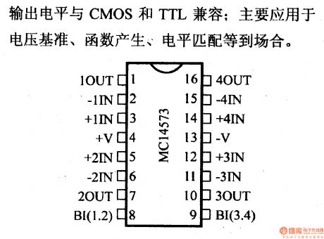
The power supply is -0.5 ~ +18 V; the input Voltage is -0.5 ~~ V +0.5 V; input current (DC ) is 10mA; operating voltage can be as low as ± 1.5V; output level is compatible with CMOS and TTL; it is mainly used in voltage reference, function generator and level matching occasions.
(View)
View full Circuit Diagram | Comments | Reading(840)
MC1437/1537 double-pass op amp and its pin main characteristics
Published:2013/1/21 0:29:00 Author:Ecco | Keyword: double-pass op amp , pin main characteristics
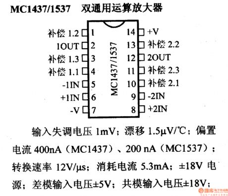
1mV input offset voltage; 1.5μV/℃ drift; bias current is 400nA ( MC1437 ) or 200nA ( MC1537 ; conversion rate is 12V/μs; Current consumption is 5.3mA; power supply is ± 18V; differential-mode input voltage is ± 5V; common-mode input voltage is ± 18V; power consumption is 625mW.
(View)
View full Circuit Diagram | Comments | Reading(1149)
NE538 high - speed operational amplifier and its pin main characteristics
Published:2013/1/21 0:36:00 Author:Ecco | Keyword: high - speed, operational amplifier, pin main characteristics
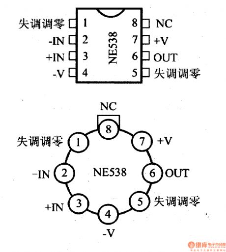
Input offset voltage is 2mV; temperature drift is 6μV / ℃; bias current is 65nA; Gain Bandwidth Product GB = 6MHz; conversion rate is 60V/μs; noise is 30nV / √ ¯ Hz (1kHz); Current consumption is 2mA; power supply is ± 18V; differential-mode input voltage is ± 30V; common-mode input voltage is ± 15V; power is 800mW.
(View)
View full Circuit Diagram | Comments | Reading(806)
NE5532 / A dual low-noise op amp and its pin main characteristics
Published:2013/1/21 0:41:00 Author:Ecco | Keyword: dual low-noise op amp , pin main characteristics
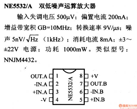
Input offset voltage is 500μV; bias current is 200nA; Gain Bandwidth Product GB = 10MHz; conversion rate is 9V/μs; noise is 5nV / √ ¯ Hz ( 1kHz); Current consumption is 8mA ; ± 3 to ± 22V power supply; power is 1000mW. Similar models: NNJM4432.
(View)
View full Circuit Diagram | Comments | Reading(2549)
NE5534 / A low-noise op amp and its pin main characteristics
Published:2013/1/21 0:45:00 Author:Ecco | Keyword: low-noise op amp , pin main characteristics

Input offset voltage is 500μV; temperature drift is 4μV / ℃; bias current is 400nA; Gain Bandwidth Product GB = 10MHz; conversion rate is 13V/μs; noise is 3.5nV / √ ¯ Hz ( 1kHz); Current consumption is 4.5mA; ± 3 ~ ± 22V power; power is 800mW.
(View)
View full Circuit Diagram | Comments | Reading(1470)
NJM2043 dual low-noise op amp and its pin main characteristics
Published:2013/1/21 0:49:00 Author:Ecco | Keyword: dual low-noise , op amp , pin main characteristics
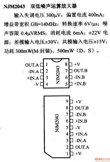
Input offset voltage is 300μV; bias current is 400nA; Gain Bandwidth Product GB = 14MH ; conversion rate is 6V/μs; noise is 0.4μVRMS; Current consumption is 6mA; power supply is ± 22V; differential-mode input voltage is ± 30V; common-mode input voltage is ± 15V; reactive consumption is 300mW (M package ), 500mW ( D , S ).
(View)
View full Circuit Diagram | Comments | Reading(1147)
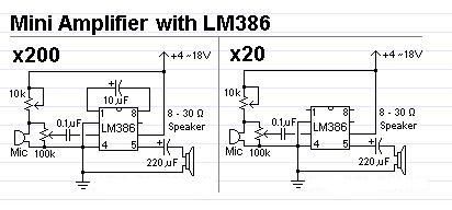
Mini Amplifier with LM386
Published:2013/1/21 0:39:00 Author:muriel | Keyword: Mini Amplifier, LM386
View full Circuit Diagram | Comments | Reading(2215)
NE5535 dual op amp and its pin main characteristics
Published:2013/1/18 2:51:00 Author:Ecco | Keyword: dual op amp , pin main characteristics
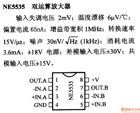
Input offset voltage is 2mV; temperature drift is 6μV / ℃; bias current is 65nA; Gain Bandwidth Product is 1MHz; conversion rate is 15V/μs; noise is 30nV / √ ¯ Hz ( 1kHz); current consumption is 3.6mA; power supply is ± 18V; differential-mode input voltage is ± 30V; common-mode input voltage is ± 15V.
(View)
View full Circuit Diagram | Comments | Reading(1415)
NJM2058 four general purpose operational amplifier and its pin main characteristics
Published:2013/1/18 2:44:00 Author:Ecco | Keyword: four general purpose, operational amplifier , pin main characteristics
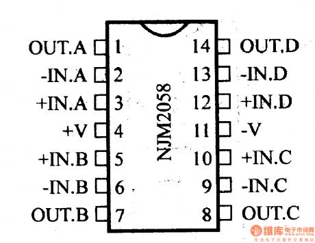
The input offset voltage is 500μV; bias current is 50nA; conversion rate is 1V/μs; noise is 25μVRMS; Current consumption is 7mA; power supply is ± 18V; differential-mode input voltage is ± 30V; common-mode input voltage is ± 15V; power is 700mW.
(View)
View full Circuit Diagram | Comments | Reading(739)
NJM2060 four wideband op amp and its pin main characteristics
Published:2013/1/18 2:55:00 Author:Ecco | Keyword: four wideband op amp , pin main characteristics
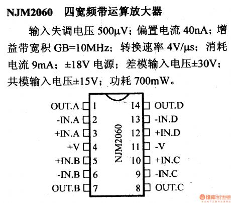
The input offset voltage is 500μV; bias current is 40nA; gain bandwidth product is 10MHz; conversion rate is 4V/μs; Current consumption is 9mA; power supply is ± 18V; differential-mode input voltage is ± 30V; common-mode input voltage is ± 15V; power is 700mW.
(View)
View full Circuit Diagram | Comments | Reading(1057)
NJM2068 dual low-noise op amp and its pin main characteristics
Published:2013/1/18 2:41:00 Author:Ecco | Keyword: dual low-noise, op amp , pin main characteristics
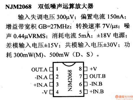
Input offset voltage 300μV; bias current is 150nA; Gain Bandwidth Product GB = 27MHz; conversion rate is 7V/μs; noise is 0.44μVRMS; Current consumption is 5mA; power supply is ± 18V; differential-mode input voltage is ± 15V; common-mode input voltage is ± 30V; power consumption is 300MW (M ), 500mW (D , S ).
(View)
View full Circuit Diagram | Comments | Reading(1761)
High-precision JFET input op amp OP-15 and its pin main characteristics
Published:2013/1/18 2:35:00 Author:Ecco | Keyword: High-precision, JFET input , op amp , pin main characteristics
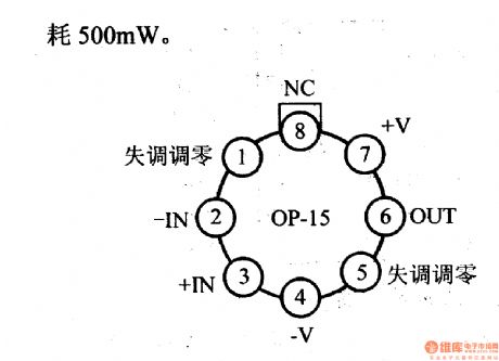
The input offset voltage is 2mV; temperature drift is 2μV / ℃; bias current is 15pA; gain bandwidth product is 6MHz; conversion rate is 13V/μs; Current consumption is 4mA; ± 22V power supply ( 15E / F ), ± 16V (15G ); power is 500mW.
(View)
View full Circuit Diagram | Comments | Reading(593)
MAX4102/MAX4103 high - speed video op amp and its pin main characteristics
Published:2013/1/17 2:07:00 Author:Ecco | Keyword: high - speed , video op amp , pin main characteristics
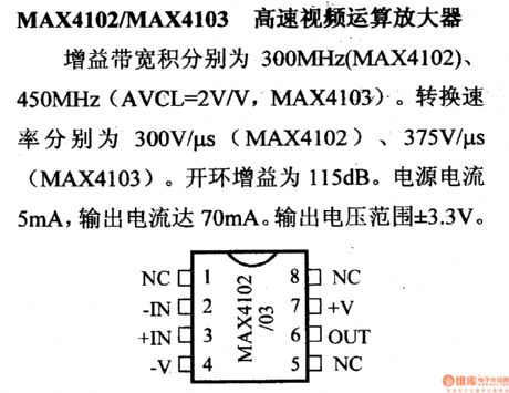
Gain bandwidth is 300MHz (MAX4102), 450MHz (AVCL = 2V / V, MAX4103). Conversion rate is 300V/μs ( MAX4102 ), 375V/μs ( MAX4103 ). The open-loop gain is 115dB. Supply current is 5mA, output current is 70mA. Output voltage range is ± 3.3V.
(View)
View full Circuit Diagram | Comments | Reading(721)
MAX4104/MAX4105 ultra- high-speed and low - noise op amp and its pin main characteristics
Published:2013/1/17 2:03:00 Author:Ecco | Keyword: ultra- high-speed , low - noise, op amp , pin main characteristics
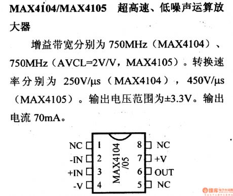
Gain bandwidth is 750MHz (MAX4104), 750MHz (AVCL = 2V / V, MAX4105). Conversion rate is 250V/μs (MAX4104), 450V/μs (MAX4105). Output voltage range is ± 3.3V. The output current is 70mA.
(View)
View full Circuit Diagram | Comments | Reading(574)
MAX475 op amp and its pin main features
Published:2013/1/17 1:43:00 Author:Ecco | Keyword: op amp, pin main features
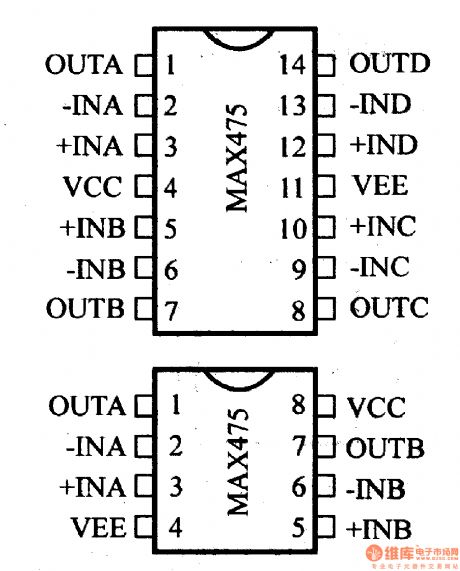
Operating voltage range is 2.7 to 5.25V; conversion rate is 15V/μs; unity gain bandwidth is 10MHz; each op amp supply current is 2mA; output swing is ± 50mV; CMRR = 90dB; PSRR = 90dB.
(View)
View full Circuit Diagram | Comments | Reading(709)
MAX492/MAX495 single-supply op amp and its pin main characteristics
Published:2013/1/17 1:57:00 Author:Ecco | Keyword: single-supply op amp, pin main characteristics
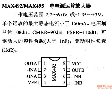
The operating voltage range is 2.7 ~ 6V or ± 1.35 ~ ± 3V. Single op amp's maximum quiescent current is less than 150mA. Voltage gain is 108dB. CMRR = 90dB, PSRR = 110dB. It can drive large capacitive load (> 1nF ) and a resistive load ( 1kΩ ).
(View)
View full Circuit Diagram | Comments | Reading(682)
MAX951-954 operational amplifier and its pin main characteristics
Published:2013/1/17 1:52:00 Author:Ecco | Keyword: operational amplifier , pin main characteristics
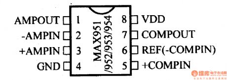
Supply voltage range is 2.2 to 7.0V; the bandwidth of MAX952/954 is 200kHz; conversion rate is 100V/ms; gain is greater than or equal to 10V / V; it contains comparator.
(View)
View full Circuit Diagram | Comments | Reading(709)
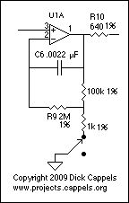
the first amplfier
Published:2013/1/16 2:12:00 Author:muriel | Keyword: amplfier
View full Circuit Diagram | Comments | Reading(605)
| Pages:22/250 At 202122232425262728293031323334353637383940Under 20 |
Circuit Categories
power supply circuit
Amplifier Circuit
Basic Circuit
LED and Light Circuit
Sensor Circuit
Signal Processing
Electrical Equipment Circuit
Control Circuit
Remote Control Circuit
A/D-D/A Converter Circuit
Audio Circuit
Measuring and Test Circuit
Communication Circuit
Computer-Related Circuit
555 Circuit
Automotive Circuit
Repairing Circuit
