TLP197A, TLP197D, TLP197GA Selling Leads, Datasheet
MFG:TOS Package Cooled:SOP-6 D/C:07+

TLP197A, TLP197D, TLP197GA Datasheet download

Part Number: TLP197A
MFG: TOS
Package Cooled: SOP-6
D/C: 07+


MFG:TOS Package Cooled:SOP-6 D/C:07+
TLP197A, TLP197D, TLP197GA Datasheet download
MFG: TOS
Package Cooled: SOP-6
D/C: 07+

Want to post a buying lead? If you are not a member yet, please select the specific/related part number first and then fill the quantity and your contact details in the "Request for Quotation Form" on the left, and then click "Send RFQ".Your buying lead can then be posted, and the reliable suppliers will quote via our online message system or other channels soon.
TOP
PDF/DataSheet Download
Datasheet: TLP
File Size: 345950 KB
Manufacturer: STMicroelectronics
Download : Click here to Download
PDF/DataSheet Download
Datasheet: TLP
File Size: 345950 KB
Manufacturer: STMicroelectronics
Download : Click here to Download
PDF/DataSheet Download
Datasheet: TLP197GA
File Size: 191075 KB
Manufacturer: TOSHIBA [Toshiba Semiconductor]
Download : Click here to Download
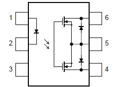
The TLP197A has the following features including 6 pin SOP (2.54SOP6) : 2.1 mm high, 2.54 mm pitch;1-Form-A;Peak Off-State Voltage : 60 V (MIN.) ;Trigger LED Current : 3 mA (MAX.) ;On-State Current : 400 mA (MAX.);Isolation Voltage : 1500 Vrms (MIN.).
The TOSHIBA TLP197A consists of an aluminum gallium arsenide infrared emitting diode optically coupled to a photo-MOS FET in a SOP, which is suitable for surface mount assembly.The TLP197A is suitable for replacement of mechanical relays in many applications which require space savings.Gallium arsenide (GaAs) is a substance used in the products described in this document. GaAs dust and fumes are toxic. Do not break, cut or pulverize the product, or use chemicals to dissolve them. When disposing of the products, follow the appropriate regulations. Do not dispose of the products with other industrial waste or with domestic garbage. The information contained herein is presented only as a guide for the applications of our products. No responsibility is assumed by TOSHIBA CORPORATION for any infringements of intellectual property or other rights of the third parties which may result from its use. No license is granted by implication or otherwise under any intellectual property or other rights of TOSHIBA CORPORATION or others.
TOSHIBA is continually working to improve the quality and reliability of its products.Nevertheless, semiconductor devices in general can malfunction or fail due to their inherent electrical sensitivity and vulnerability to physical stress. It is the responsibility of the buyer, when utilizing TOSHIBA products, to comply with the standards of safety in making a safe design for the entire system, and to avoid situations in which a malfunction or failure of such TOSHIBA products could cause loss of human life, bodily injury or damage to property. In developing your designs, please ensure that TOSHIBA products are used within specified operating ranges as set forth in the most recent TOSHIBA products specifications. Also, please keep in mind the precautions and conditions set forth in the "Handling Guide for Semiconductor Devices," or "TOSHIBA Semiconductor Reliability Handbook" etc.
The Toshiba TLP197D consists of an aluminum gallium arsenide infrared emitting diode optically coupled to a photo-MOSFET in a SOP package.
TLP197D is housed in a compact and thin SOP package and has characteristics of high-withstanding voltage and low ON-state resistance, which enable TLP197D to be applied in hook switches, dial-pulse switches for modems and facsimiles, and switches for test circuit switching in PBXes.
| Characteristics | Symbol | Rating | Unit | ||
| LED | Forward current | IF | 50 | mA | |
| Forward current derating (Ta 25°C) |
IF/°C | -0.5 | mA/°C | ||
| Pulse forward current (100 s pulse, 100 pps) |
IFP | 1 | A | ||
| Reverse voltage | VR | 5 | V | ||
| Junction temperature | Tj | 125 | °C | ||
| Detector | Off-state output terminal voltage | VOFF | 200 | V | |
| On-state current | A connection | ION | 200 | mA | |
| B connection | 200 | ||||
| C connection | 400 | ||||
| On-state current derating (Ta => 25°C) |
A connection | ION/°C | -2.0 | mA/°C | |
| B connection | -2.0 | ||||
| C connection | -4.0 | ||||
| Junction temperature | Tj | 125 | °C | ||
| Storage temperature range | Tstg | -55 to 125 | °C | ||
| Operating temperature range | Topr | -40 to 85 | °C | ||
| Lead soldering temperature (10 s) | Tsol | 260 | °C | ||
| Isolation voltage (AC, 1 min., R.H. 60%) (Note 1) |
BVS | 1500 | Vrms | ||
Note: Using continuously under heavy loads (e.g. the application of high temperature/current/voltage and the significant change in temperature, etc.) may cause this product to decrease in the reliability significantly even if the operating conditions (i.e. operating temperature/current/voltage, etc.) are within the absolute maximum ratings.
Please design the appropriate reliability upon reviewing the Toshiba Semiconductor Reliability Handbook ("Handling Precautions"/"Derating Concept and Methods") and individual reliability data (i.e. reliability test report and estimated failure rate, etc).
Note 1: Pins 1, 2 and 3 are shorted together, and pins 4, 5 and 6 are shorted together.

The TOSHIBA TLP197GA consists of an aluminum gallium arsenide infrared emitting diode optically coupled to a photo-MOSFET in a SOP,which is suitable for surface mount assembly.
The TLP197GA is suitable for replacement of mechanical relays in many applications which require space savings.
• 6 pin SOP (2.54SOP6): 2.1 mm high, 2.54 mm pitch
• 1-form-A
• Peak off-state voltage: 400 V (min)
• Trigger LED current: 3 mA (max)
• On-state current: 120 mA (max)
• On-state resistance: 35 (max)
• Isolation voltage: 1500 Vrms (min)
• BSI approved: BS EN60065:2002, certificate no.8753
BS EN60950-1:2002, certificate no.8754
|
Characteristics
|
Symbol |
Rating |
Unit | ||
| LED | Forward current |
IF |
50 |
mA | |
| Forward current derating (Ta 25°C) |
IF/°C |
-0.5 |
mA/°C | ||
| Peak forward current (100 s pulse, 100 pps) |
IFP |
1 |
A | ||
| Reverse voltage |
VR |
5 |
V | ||
| Junction temperature |
Tj |
125 |
°C | ||
| Detector | Off-state output terminal voltage |
VOFF |
400 |
V | |
| On-state current | A connection |
ION |
120 |
mA | |
| B connection |
120 | ||||
| C connection |
240 | ||||
| On-state current derating (Ta 25°C) |
A connection |
ION/°C |
-1.2 |
mA/°C | |
| B connection |
-1.2 | ||||
| C connection |
-2.4 | ||||
| Junction temperature |
Tj |
125 |
°C | ||
| Operating temperature range |
Topr |
−40 to 85 |
°C | ||
| Storage temperature range |
Tstg |
−55 to 125 |
°C | ||
| Lead soldering temperature (10 s) |
Tsol |
260 |
°C | ||
| Isolation voltage (AC, 1 min, R.H. <= 60%) (Note 1) |
BVS |
1500 |
Vrms | ||
Note: Using continuously under heavy loads (e.g. the application of high temperature/current/voltage and the significant change in temperature, etc.) may cause this product to decrease in the reliability significantly even if the operating conditions (i.e. operating temperature/current/voltage, etc.) are within the absolute maximum ratings.Please design the appropriate reliability upon reviewing the Toshiba Semiconductor Reliability Handbook ("Handling Precautions"/"Derating Concept and Methods") and individual reliability data (i.e. reliability test report and estimated failure rate, etc).
Note 1: Device considered a two-terminal device: LED side pins shorted together, and DETECTOR side pins shorted together.

Price: 4-6 USD
MT58L64L18CT-10 TQFP100

Price: 5-6.5 USD
DL-7140-211M laser tube

Price: 4-5 USD
74LVC74APG - IC FLIP FLOP D-Type POS-EDG DUAL 14TSSOP

Price: 6.5-8 USD
CYPRESS - Clock Synthesizer with Differential CPU Outputs

Price: 0.284-0.286 USD
PI5V330QEX Pericom Multiplexer Switch ICs

Price: 1-2 USD
IGBT power module, Single switch, 1200 V, Collector-emitter voltage, 430A

Price: 1-2 USD
a-Si TFT-LCD, NEC, 228.096Hmm, 560V

Price: 0.124-0.2 USD
PC354N1T - Mini-flat Package, AC Input Type Photocoupler - Sharp Electrionic Components

Price: 0.177-0.178 USD
RL1210JR51-XX-BL - Thick Film Chip Resistor Low Ohmic - TAITRON Components Incorporated

Price: 0.053-0.055 USD
STPS140A - POWER SCHOTTKY RECTIFIER - STMicroelectronics

Price: 1.45-1.5 USD
STA013 - MPEG 2.5 LAYER III AUDIO DECODER - STMicroelectronics

Price: 0.073-0.075 USD
SMBJ5347B - 5 Watt Surface Mount Silicon Zener Diodes - Micro Commercial Components
