Want to post a buying lead? If you are not a member yet, please select the specific/related part number first and then fill the quantity and your contact details in the "Request for Quotation Form" on the left, and then click "Send RFQ".Your buying lead can then be posted, and the reliable suppliers will quote via our online message system or other channels soon.
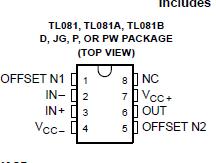
The TL08_ JFET-input operational amplifier family is designed to offer a wider selection than any previously developed operational amplifier family. Each of these JFET-input operational amplifiers incorporates well-matched, high-voltage JFET and bipolar transistors in a monolithic integrated circuit. The devices feature high slew rates, low input bias and offset currents, and low offset voltage temperature coefficient. Offset adjustment and external compensation options are available within the TL08_ family.
Device types with a C suffix are characterized for operation from 0 to 70, those with an I suffix are characterized for operation from 40°C to 85, and those with an M suffix are characterized for operation over the full military temperature range of 55 to 125.
TL081A Maximum Ratings
TL08_C TL08_AC TL08_BC
TL08_I
TL08_M
UNIT
Supply voltage, VCC+ (see Note 1)
18
18
18
V
ply voltage VCC (see Note 1)
18
18
18
V
Differential input voltage (see Note 2)
± 30
± 30
± 30
V
Input voltage (see Notes 1 and 3)
±15
±15
±15
V
Duration of output short circuit (see Note 4)
unlimited
unlimited
unlimited
Continuous total dissipation
See Dissipation Rating Table
Operating free-air temperature range
0 to 70
40 to 85
55 to 125
Storage temperature range
65 to 150
65 to 150
65 to 150
Case temperature for 60 seconds
FK package
260
Lead temperature 1,6 mm (1/16 inch) from case for 60 seconds
Jor JG package
300
Lead temperature 1,6 mm (1/16 inch) from case for 10 seconds
D,N,P,or PW package
260
260
NOTES: 1. All voltage values, except differential voltages, are with respect to the midpoint between VCC+ and VCC. 2. Differential voltages are at the noninverting input terminal with respect to the inverting input terminal. 3. The magnitude of the input voltage must never exceed the magnitude of the supply voltage or 15 V, whichever is less. 4. The output may be shorted to ground or to either supply. Temperature and/or supply voltages must be limited to ensure that the dissipation rating is not exceeded.
TL081A Features
• Low-Power Consumption • Wide Common-Mode and Differential Voltage Ranges • Low Input Bias and Offset Currents • Output Short-Circuit Protection • Low Total Harmonic Distortion . . . 0.003% Typ • High Input Impedance . . . JFET-Input Stage • Internal Frequency Compensation (Except TL080, TL080A) • Latch-Up-Free Operation • High Slew Rate . . . 13 V/ms Typ • Common-Mode Input Voltage Range Includes VCC+