TC4001BFNELPNSM, TC4001BFT, TC4001BP Selling Leads, Datasheet
MFG:TOSHIBA Package Cooled:105000 D/C:88+

TC4001BFNELPNSM, TC4001BFT, TC4001BP Datasheet download

Part Number: TC4001BFNELPNSM
MFG: TOSHIBA
Package Cooled: 105000
D/C: 88+


MFG:TOSHIBA Package Cooled:105000 D/C:88+

TC4001BFNELPNSM, TC4001BFT, TC4001BP Datasheet download

MFG: TOSHIBA
Package Cooled: 105000
D/C: 88+
Want to post a buying lead? If you are not a member yet, please select the specific/related part number first and then fill the quantity and your contact details in the "Request for Quotation Form" on the left, and then click "Send RFQ".Your buying lead can then be posted, and the reliable suppliers will quote via our online message system or other channels soon.
TOP
PDF/DataSheet Download
Datasheet: TC4001
File Size: 197001 KB
Manufacturer: TOSHIBA [Toshiba Semiconductor]
Download : Click here to Download
PDF/DataSheet Download
Datasheet: TC4001BFT
File Size: 197001 KB
Manufacturer: TOSHIBA [Toshiba Semiconductor]
Download : Click here to Download
PDF/DataSheet Download
Datasheet: TC4001BP
File Size: 197001 KB
Manufacturer: TOSHIBA [Toshiba Semiconductor]
Download : Click here to Download
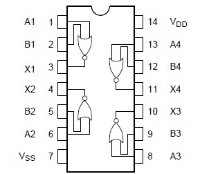
The TC4001B is 2-input positive NOR gate, respectively. Since the outputs of these gates are equipped with the buffers, the input/output transmission characteristics have been improved and the variation of transmission time due to an increase in the load capacity is kept minimum.
DC supply voltage VDD ...............VSS − 0.5 to VSS + 20 V
Input voltage VIN ......................VSS − 0.5 to VDD + 0.5 V
Output voltage VOUT ................VSS − 0.5 to VDD + 0.5 V
DC input current IIN ............................................±10 mA
Power dissipation PD ..............300 (DIP)/180 (SOIC) mW
Operating temperature range Topr .............−40 to 85
Storage temperature range Tstg ...............−65 to 150
Note: Exceeding any of the absolute maximum ratings, even briefly, lead to deterioration in IC performance or even destruction.
Using continuously under heavy loads (e.g. the application of high temperature/current/voltage and the significant change in temperature, etc.) may cause this product to decrease in the reliability significantly even if the operating conditions (i.e. operating temperature/current/voltage, etc.) are within the absolute maximum ratings and the operating ranges. Please design the appropriate reliability upon reviewing the Toshiba Semiconductor Reliability Handbook ("Handling Precautions"/"Derating Concept and Methods") and individual reliability data (i.e. reliability test report and estimated failure rate, etc).

