M74HC651, M74HC651B1, M74HC651B1N Selling Leads, Datasheet
MFG:ST Package Cooled:DIP D/C:00-99

M74HC651, M74HC651B1, M74HC651B1N Datasheet download

Part Number: M74HC651
MFG: ST
Package Cooled: DIP
D/C: 00-99


MFG:ST Package Cooled:DIP D/C:00-99

M74HC651, M74HC651B1, M74HC651B1N Datasheet download

MFG: ST
Package Cooled: DIP
D/C: 00-99
Want to post a buying lead? If you are not a member yet, please select the specific/related part number first and then fill the quantity and your contact details in the "Request for Quotation Form" on the left, and then click "Send RFQ".Your buying lead can then be posted, and the reliable suppliers will quote via our online message system or other channels soon.
TOP
PDF/DataSheet Download
Datasheet: M74HC651
File Size: 207311 KB
Manufacturer: STMicro
Download : Click here to Download
PDF/DataSheet Download
Datasheet: M74HC651B1R
File Size: 207311 KB
Manufacturer: STMICROELECTRONICS [STMicroelectronics]
Download : Click here to Download
PDF/DataSheet Download
Datasheet: M74AC574B
File Size: 83392 KB
Manufacturer: STMICROELECTRONICS [STMicroelectronics]
Download : Click here to Download
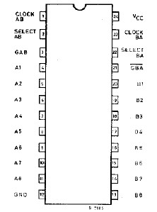
M74HC651/652 are high speed CMOS OCTAL BUS TRANSCEIVERS AND REGISTERS (3- STATE), fabricated in silicon gate C2MOS technology. They have the same high speed performance of LSTTL combined with trueCMOSlow power consumption. These devices consist of bus transceiver circuits, D-type flip-flops, and control circuitry arranged for multiplexed transmission of data directly from the input bus or from the internal storage registers. EnableGABand GBA are provided to control the transceiver functions.
Select AB and Select BA control pins are provided to select whether real-time or stored data is transfered. A low input level selects real-time data, and a high selects stored data.
Data on the Aor B bus, or both, can be stored in the internal D flip-flops by low-to-high transitions at the appropriate clock pins (CLOCK AB or CLOCK BA) regardless of the select or enable control pins. When select AB and select BA are in the real-time transfer mod e, it is also possible to store data without using the internal D-type flip-flops by simultaneously enablingGAB and GBA. In this configuration each output reinforces its input. Thus, when all other data sources to the two sets of bus lines are at high impedance, each set of bus lines will remain at its last state. All inputs are equipped with protection circuits against static discharge and transient excess voltage.
|
Symbol |
Parameter |
Value |
Unit |
|
VCC |
Supply Voltage |
-0.5 to +7 |
V |
|
VI |
DC Input Voltage |
-0.5 to VCC + 0.5 |
V |
|
VO |
DC Output Voltage |
-0.5 to VCC + 0.5 |
V |
|
IIK |
DC Input Diode Current |
± 20 |
mA |
|
IOK |
DC Output Diode Current |
± 20 |
mA |
|
IO |
DC Output Source Sink Current Per Output Pin |
± 35 |
mA |
|
ICC or IGND |
DC VCC or Ground Current |
± 70 |
mA |
|
PD |
Power Dissipation |
500 (*) |
mW |
|
Tstg |
Storage Temperature |
-65 to +150 |
°C |
|
TL |
Lead Temperature (10 sec) |
300 |
°C |

